Section 8 I/O Ports
Rev. 7.00 Mar 10, 2005 page 198 of 652
REJ09B0042-0700
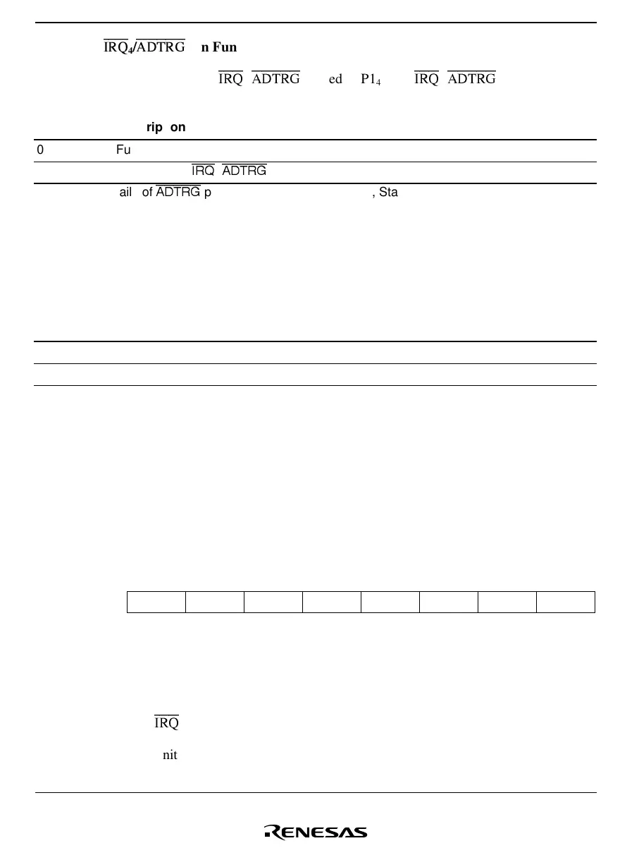
Bit 4—P1
4
/
IRQ
4
/
ADTRG
Pin Function Switch (IRQ4)
This bit selects whether pin P1
4
/
IRQ
4
/
ADTRG
is used as P1
4
or as
IRQ
4
/
ADTRG
.
Bit 4
IRQ4 Description
0 Functions as P1
4
I/O pin (initial value)
1 Functions as
IRQ
4
/
ADTRG
input pin
Note: For details of
ADTRG
pin setting, see section 12.3.2, Start of A/D Conversion by External
Trigger Input.
Bit 3—P1
3
/TMIG Pin Function Switch (TMIG)
This bit selects whether pin P1
3
/TMIG is used as P1
3
or as TMIG.
Bit 3
TMIG Description
0 Functions as P1
3
I/O pin (initial value)
1 Functions as TMIG input pin
Bits 2 and 0—Reserved
These bits are reserved; they can only be written with 0.
Bit 1—Reserved
This bit is reserved; it is always read as 1 and cannot be modified.
Port Mode Register 2 (PMR2)
Bit 76543210
— — POF1 — — WDCKS NCS IRQ0
Initial value 1 1 0 1 1 0 0 0
Read/Write — — R/W — — R/W R/W R/W
PMR2 is an 8-bit read/write register. It controls whether the PMOS transistor internal to P3
5
is on
or off, the selection of the watchdog timer clock, the selection of TMIG noise cancellation, and
switching of the P4
3
/
IRQ
0
pin functions.
Upon reset, PMR2 is initialized to H'D8.

 Loading...


