Rev. 7.00 Mar 10, 2005 page xxvi of xlii
Item Page Revision (See Manual for Details)
16.8.2 DC
Characteristics
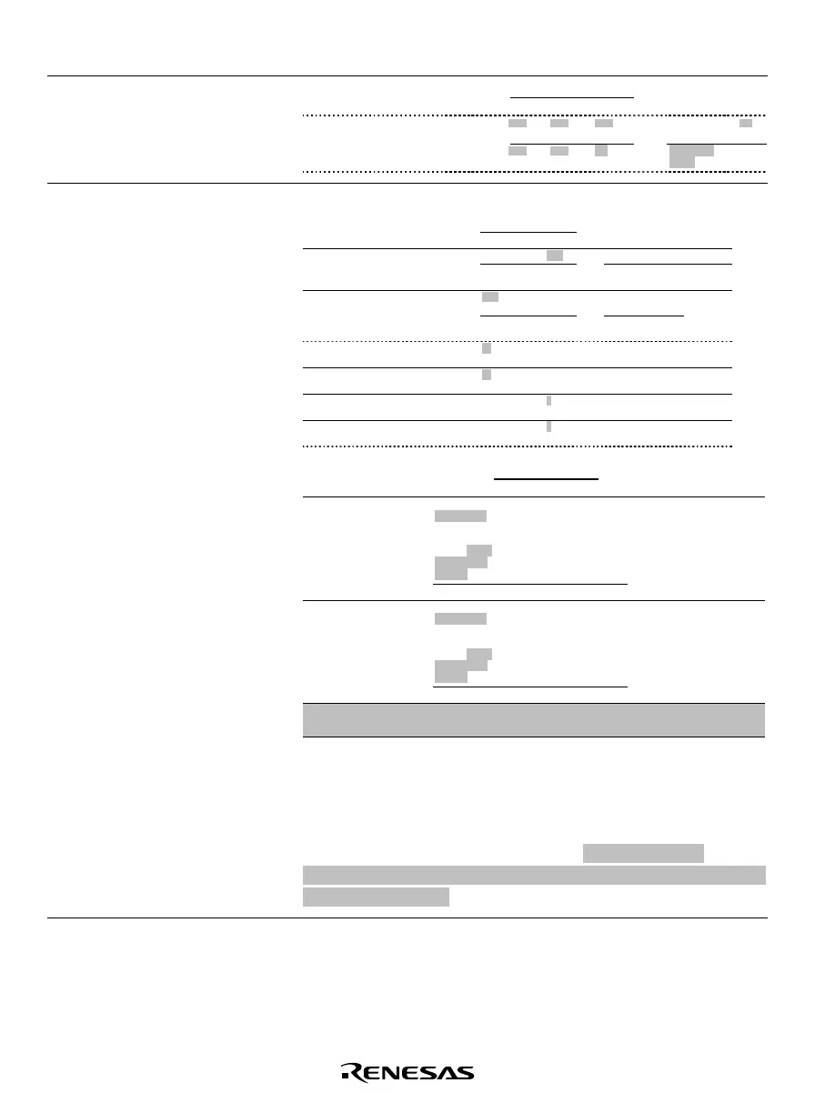
Table 16.21 DC
Characteristics
517
Values
Item Symbol
Applicable
Pins Min Typ Max Unit
Test
Condition Notes
Allowable output low
current (per pin)
I
OL
Port 9 ——15.0 mA
V
CC
= 4.0 V to
5.5 V
——5.0
Other than
above
16.8.3 AC
Characteristics
Table 16.22 Control
Signal Timing
519, 520 Table and notes amended
Values
Item Symbol
Applicable
Pins
Min Typ Max Unit Test Condition
Reference
Figure
f
OSC
OSC
1
, OSC
2
2.0 — 20.0 MHzSystem clock
oscillation
frequency
0.7 — 2.0 On-chip oscillator
selected
*
2
OSC clock (φ
OSC
)
cycle time
t
OSC
OSC
1
, OSC
2
50.0 — 500 ns Figure 16.1
500 — 1429 On-chip oscillator
selected
External clock high
width
t
CPH
OSC
1
20 ——ns Figure 16.1
External clock low
width
t
CPL
OSC
1
20 ——ns Figure 16.1
External clock rise
time
t
CPr
OSC
1
—— 5 ns F igure 16.1
External clock fall
time
t
CPf
OSC
1
—— 5 ns F igure 16.1
Values
Item Symbol
Applicable
Pins Min Typ Max Unit Test Condition
Reference
Figure
Input pin high
width
t
IH
IRQ0, IRQ1,
IRQ3, IRQ4,
IRQAEC,
WKP0 to
WKP7,
TMIC,
TMIF, TMIG,
ADTRG
2 ——t
cyc
t
subcyc
Figure 16.3
AEVL, AEVH 0.5 ——t
OSC
Input pin low
width
t
IL
IRQ0, IRQ1,
IRQ3, IRQ4,
IRQAEC,
WKP0 to
WKP7,
TMIC,
TMIF, TMIG,
ADTRG
2 ——t
cyc
t
subcyc
Figure 16.3
AEVL, AEVH 0.5 ——t
OSC
UD pin minimum
transition width
t
UDH
t
UDL
UD 4 — — t
cyc
t
subcyc
Figure 16.6
2. These characteristics are given as ranges between minimum
and maximum values in order to account for factors such as
temperature, power supply voltage, and variation among
production lots. When designing systems, make sure to give
due consideration to the SPEC range. Please contact a
Renesas sales or support representative for actual performance
data on the product.

 Loading...


