Section 9 Timers
Rev. 7.00 Mar 10, 2005 page 282 of 652
REJ09B0042-0700
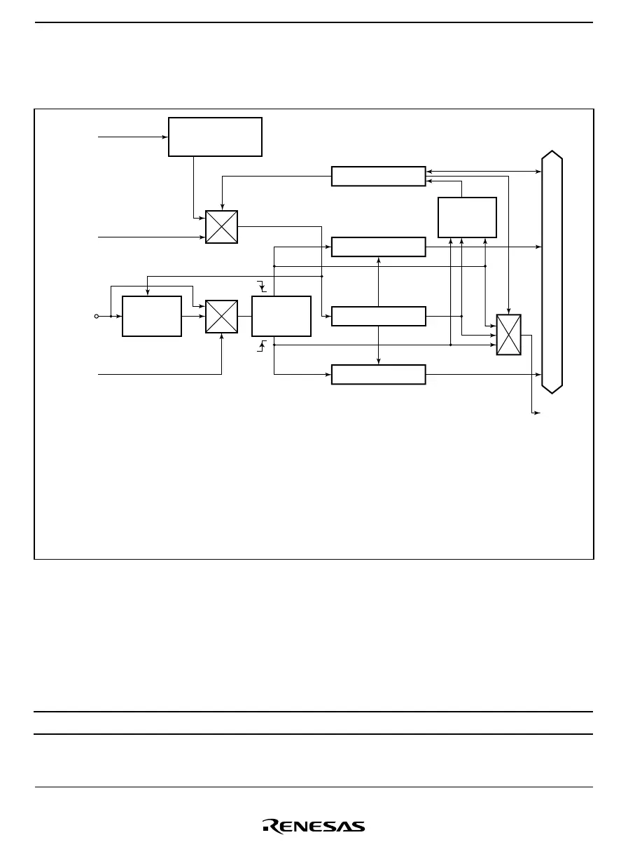
Block Diagram
Figure 9.8 shows a block diagram of timer G.
PSS
TMG
ICRGF
TCG
ICRGR
Noise
canceler
Edge
detector
Level
detector
IRRTG
φ
φ
W
/4
TMIG
NCS
[Legend]
TMG:
TCG:
ICRGF:
ICRGR:
IRRTG:
NCS:
PSS:
Timer mode register G
Timer counter G
Input capture register GF
Input capture register GR
Timer G interrupt request flag
Noise canceler select
Prescaler S
Internal data bus
Figure 9.8 Block Diagram of Timer G
Pin Configuration
Table 9.10 shows the timer G pin configuration.
Table 9.10 Pin Configuration
Name Abbr. I/O Function
Input capture input TMIG Input Input capture input pin

 Loading...


