Section 9 Timers
Rev. 7.00 Mar 10, 2005 page 287 of 652
REJ09B0042-0700
Bits 1 and 0—Clock Select (CKS1, CKS0)
Bits 1 and 0 select the clock input to TCG from among four internal clock sources.
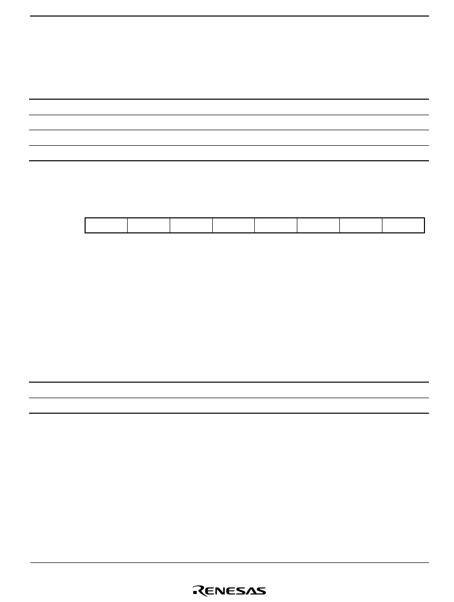
Bit 1
CKS1
Bit 0
CKS0 Description
0 0 Internal clock: counting on φ/64 (initial value)
0 1 Internal clock: counting on φ/32
1 0 Internal clock: counting on φ/2
1 1 Internal clock: counting on φw/4
Clock Stop Register 1 (CKSTPR1)
TFCKSTP TCCKSTP TACKSTP
S32CKSTP ADCKSTP TGCKSTP
76543210
1
1111111
R/W R/W R/W
R/W R/W
R/W
Bit:
Initial value:
Read/Write:
CKSTPR1 is an 8-bit read/write register that performs module standby mode control for peripheral
modules. Only the bit relating to timer G is described here. For details of the other bits, see the
sections on the relevant modules.
Bit 3—Timer G Module Standby Mode Control (TGCKSTP)
Bit 3 controls setting and clearing of module standby mode for timer G.
TGCKSTP Description
0 Timer G is set to module standby mode
1 Timer G module standby mode is cleared (initial value)

 Loading...


