Appendix B Internal I/O Registers
Rev. 7.00 Mar 10, 2005 page 585 of 652
REJ09B0042-0700
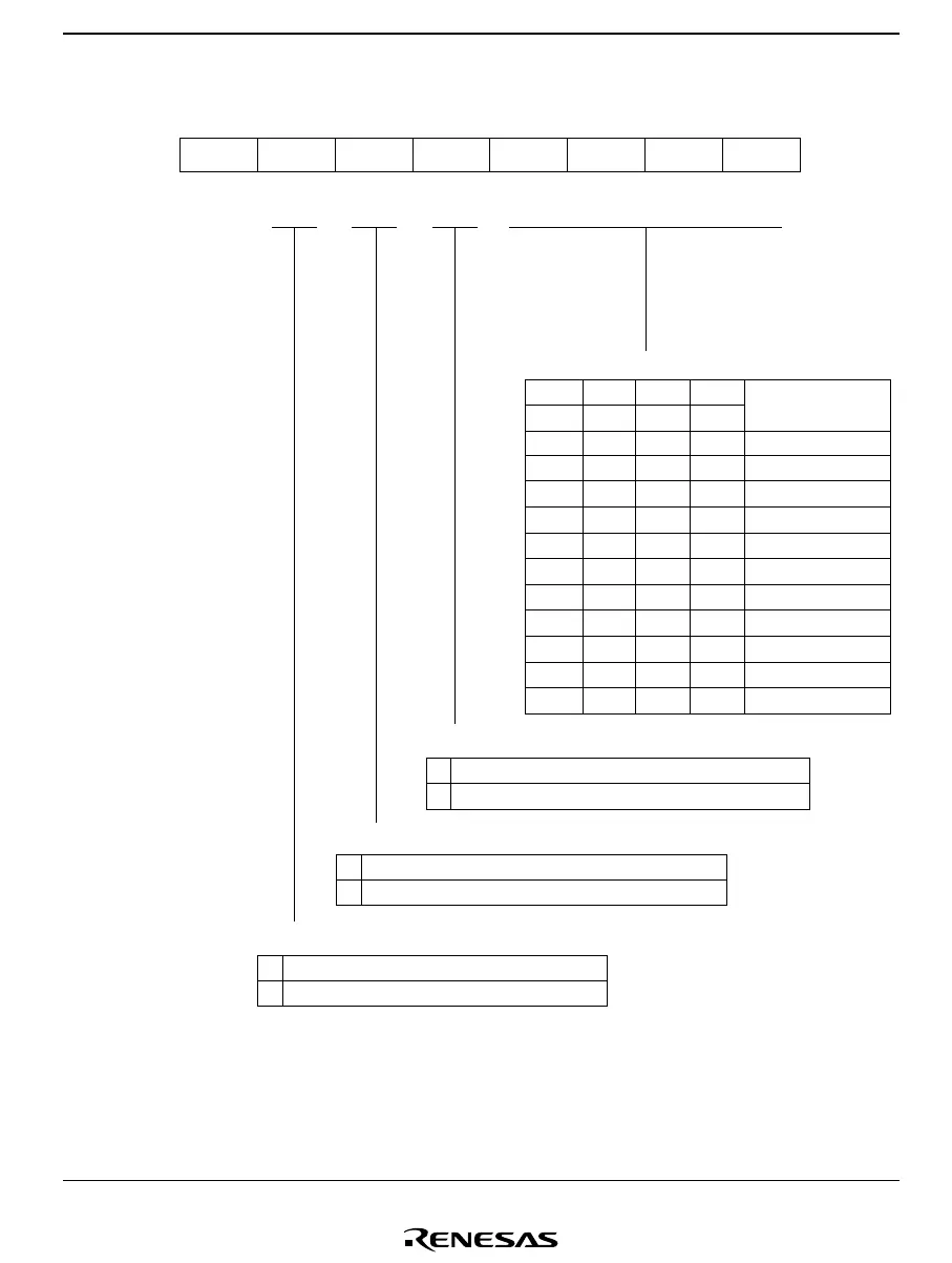
LCR—LCD Control Register H'C1 LCD Controller/Driver
Bit
Initial value
Read/Write
7
1
6
PSW
0
R/W
5
ACT
0
R/W
3
CKS3
0
R/W
0
CKS0
0
R/W
2
CKS2
0
R/W
1
CKS1
0
R/W
4
DISP
0
R/W
LCD Drive Power Supply On/Off Control
Frame Frequency Select
Operating Clock
Bit 1
Bit 2
Bit 3
0
0
0
1
1
1
1
1
1
1
1
*
*
*
0
0
0
0
1
1
1
1
0
0
1
0
0
1
1
0
0
1
1
0
1
*
0
1
0
1
0
1
0
1
Bit 1
CKS1
CKS2
CKS3
CKS0
φ
w
φ
w
/2
φ
w
/4
φ/2
φ/4
φ/8
φ/16
φ/32
φ/64
φ/128
φ/256
Display Function Activate
LCD controller/driver operation halted
LCD controller/driver operates
*: Don't care
0
1
0 LCD drive power supply off
1 LCD drive power supply on
Display Data Control
0 Blank data is displayed
1 LCD RAM data is displayed

 Loading...


