DCO Setup and Calibration
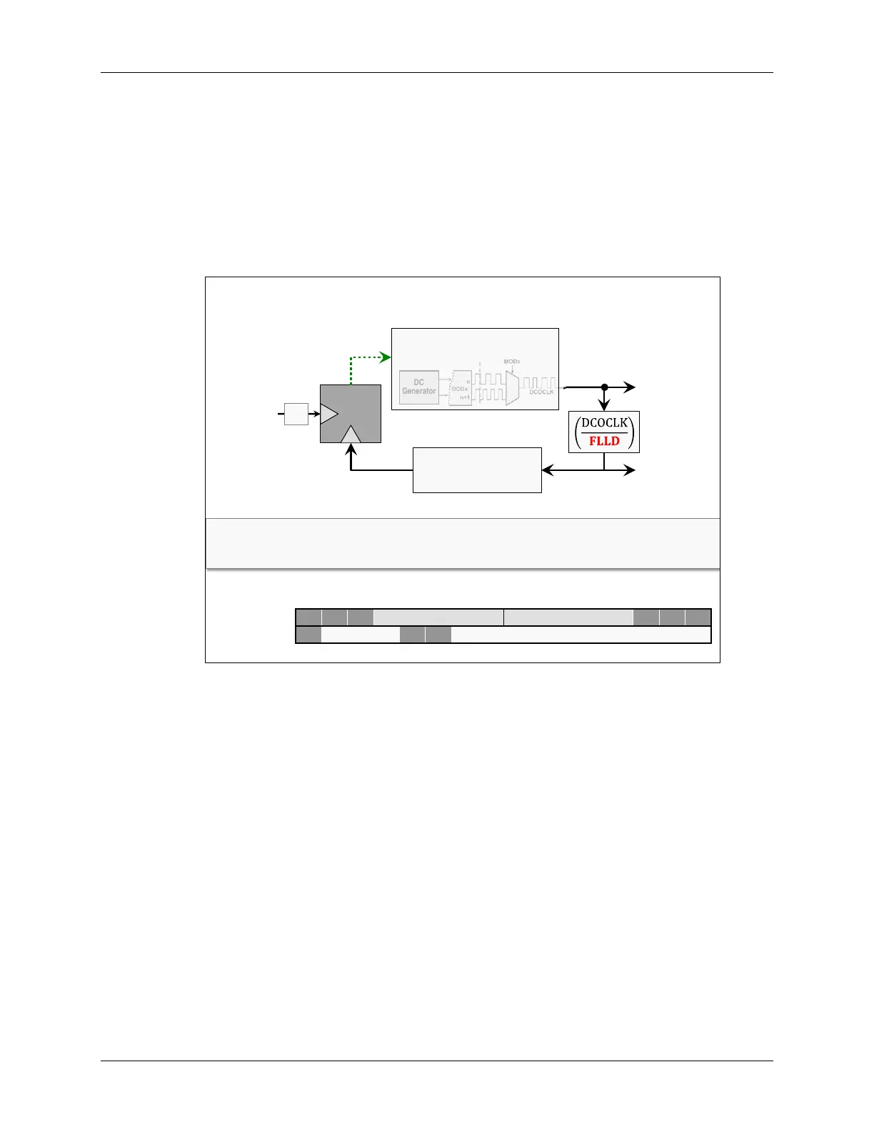
At the top center of the following diagram, you’ll see the DCO circuitry. The output of the DCO is
labeled DCOLCLK. To provide more flexibility, this signal is divided by a bit-field value called
FLLD to make up a second clock frequency called DCOCLKDIV; not only can this clock be used
to source MCLK, SMCLK or ACLK, but it is also part of the clock’s feedback stabilization.
DCOCKLDIV is divided again by the bit-field FLLN which is then fed into an integrator. Once you
have selected a reference input clock to the integrator, the FLL will tweak the MOD bits as
needed to make sure the number of DCO clock outputs correlate to the FLL reference clock.
Thus even with varying voltage and temperature, as long as the FLL reference remains stable, so
will the DCO clock.
‘F5xx Hardware FLL
UCSCTL0 DCO MOD
UCSCTL2 FLLD FLLN
15 14 13 12 11 10 9 8 7 6 5 4 3 2 1 0
DCOCLK
DCOCLKDIV
DCO and MODulator
DC
Generator
FLLREFCLK
Divider
DCOCLKDIV/(FLLN+1)
Integrator
-
+
XT1
XT2
REFO
Inc/dec DCO+MOD
bit-fields
as needed
÷n
DCOCLK = (FLLREFCLK/n) * FLLD * (FLLN + 1)
where: n = FLLREFDIV
As long as you know the desired value of DCOCLK and the FLL Reference Clock, it’s a simple
matter of choosing values for the 3 divider/multiplier fields (n, FLLD, FLLN) to solve the equation.
DCOCLK = (FLLREFCLK/n) * FLLD * (FLLN + 1)
MSP430 Workshop - MSP430 Clocks & Initialization 4 - 29