Adjuncts and Peripherals
909A/B universal coupler
834 SI Installation and Upgrades
June 2004
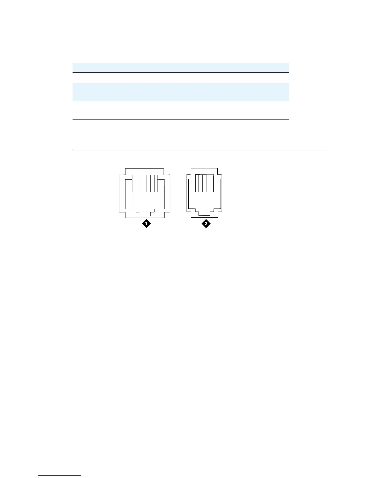
Figure 325 shows the physical locations of the pins for J1, J2, and J3.
Figure 325: Typical modular jack pinout
Table 47: J3 Pin Assignments (Power Connections)
Pin Color Designation Description
1, 3, 4, & 7 — — Not used
2 Black GRD -48 RET or ground lead from system or
from positive lead of power supply
5 Yellow -48 VDC -48 VDC from system or from negative
lead of power supply
Figure notes
1 J1 and J2 8-pin modular jacks 2 J3 7-pin modular jack
18
5
mod_jack RBP 041796
 Loading...