x/EN FD/Na7
-
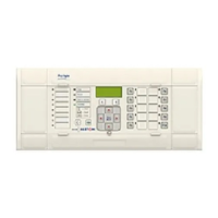
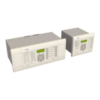
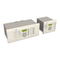
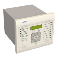
MiCOM P74
2. HARDWARE MODULES
The relay is based on a modular hardware design where each module performs a separate
function within the relay operation. This section describes the functional operation of the
various hardware modules.
2.1 Processor board
The relay is based around a TMS320VC33 floating point, 32-bit digital signal processor
(DSP) operating at a clock frequency of 75MHz. This processor performs all of the
calculations for the relay, including the protection functions, control of the data
communication and user interfaces including the operation of the LCD, keypad and LEDs.
The processor board is located directly behind the relay’s front panel which allows the LCD,
function keys and LEDs to be mounted on the processor board along with the front panel
communication ports. These comprise the 9-pin D-connector for EIA(RS)232 serial
communications (e.g. using S1 and Courier communications) and the 25-pin D-connector
relay test port for parallel communication. All serial communication is handled using a field
programmable gate array (FPGA).
All serial communication is handled using a two-channel 85C30 serial communications
controller (SCC).
The memory provided on the main processor board is split into two categories, volatile and
non-volatile; the volatile memory is fast access SRAM which is used for the storage and
execution of the processor software, and data storage as required during the processor’s
calculations. The non-volatile memory is sub-divided into 2 groups; 4MB of flash memory for
non-volatile storage of software code, present setting values, text, configuration data, latched
data signals (from control inputs, function keys, LEDs, relay outputs) and 4MB of battery
backed-up SRAM for the storage of disturbance, event, fault and maintenance record data.
2.2 Coprocessor board
The co-processor board is based around a TMS320VC5402, 16-bit digital signal processor
(DSP) operating at a clock frequency of 100MHz.
The features of the co-processor board are:
• 128 K * 16 bits high speed memory for external code execution.
• 128 K * 16 bits high speed memory for data storage.
• Interface with first interconnection bus from main board.
• 4 K * 16 bits double access memory for communication with main board.
• Interface with second interconnection bus towards peripheral boards.
• Serial communication interface on optical fibre with 4 full duplex channels. The
communication uses a synchronous protocol with a date rate of 2.5 Mbit/s.
On the co-processor board only 2 of the 4 optical channels are provided.
On board DC-DC converter which gives 3.3V chip power supply from the interconnection bus
22V rail.
After power on, the main board loads the software in coprocessor board via double access
memory. When software starts, the microprocessor configures the board. After this, optical
communication can begin.
In P741 relay, coprocessor board controls 1 opto board, 1 relay board and up to 7
communication boards via its own interconnection bus.
In P742 and P743 relays, coprocessor board controls opto boards and relay boards via its
own interconnection bus. Coprocessor board provides the sample synchronisation to input
module and receives the samples from input module.