Section 2 - Functional Description
2-25
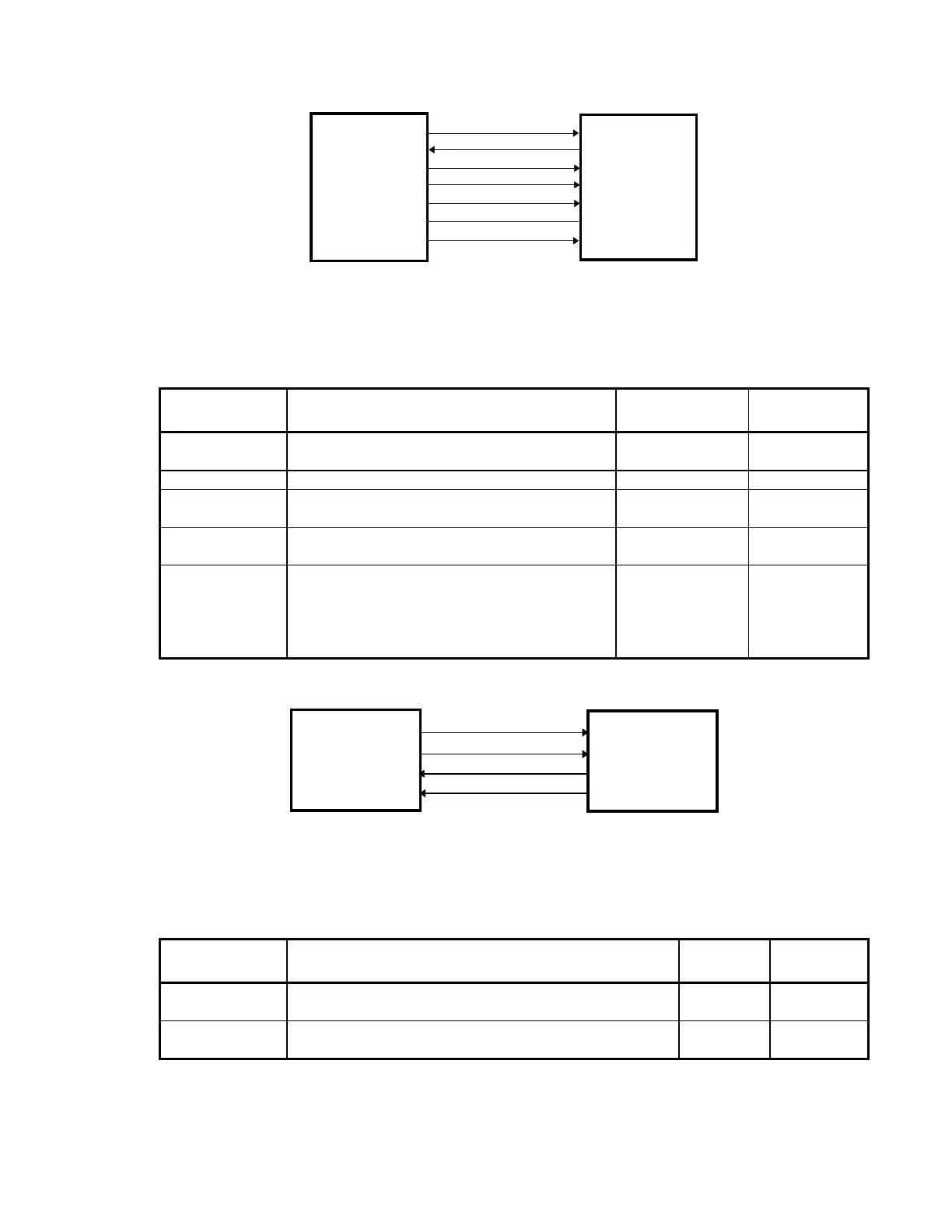
KVREF+, KVREF-
KV_CHK
78.125KHz+, 78.125khz-
XREN+, XREN-
+15V_(P)
AGND_(P)
-15V_(P)
I/O
and
LOGIC
BOARD
DUTY CYCLE
DRIVER
BOARD
Figure 2-13. I/O and Logic Board/Duty Cycle Driver Board
Interconnection Diagram
Table 2-18. I/O and Logic Board/Duty Cycle Driver Board
Interconnection Descriptions
Signal Description
IOL
Pins
DCD
Pins
kVREF+
kVREF-
Pulse Amplitude reference JP4-2
JP4-3
JP1-2
JP1-3
kVCHK Sense amplifier output signal. JP4-4 JP1-4
78.125KHZ+
78.125KHz-
Duty cycle Driver clock. JP4-5
JP4-6
JP1-5
JP1-6
XREN+
XREN-
X-Ray enabling gate. JP4-7
JP4-8
JP1-7
JP1-8
+15V_(P)
AGND_(P)
-15V_(P)
Provides power for the Duty Cycle Driver board. JP4-10, JP4-11
JP4-12, JP4-13
JP4-14, JP4-15
JP1-10, JP1-11
JP1-12, JP1-13
JP1-14, JP1-15
VAF
VBF
PRIM+
PRIM-
H-BRIDGE
BOARD
DUTY CYCLE
DRIVER
BOARD
Figure 2-14. H-Bridge Board/Duty Cycle Driver Board Interconnection
Diagram
Table 2-19. H-Bridge Board/Duty Cycle Driver Board Interconnection
Descriptions
Signal Description
H-B
Pins
DCD
Pins
VAF
VBF
Pulse amplitude feedback pulse. JP3-1
JP3-3
JP2-1
JP2-3
PRIM+
PRIM-
High Voltage Transformer drive pulse. WP1, WP2
WP3, WP4
JP4-1, JP4-2
JP4-3, JP4-4