QDR
®
4500 Technical Manual
2-28
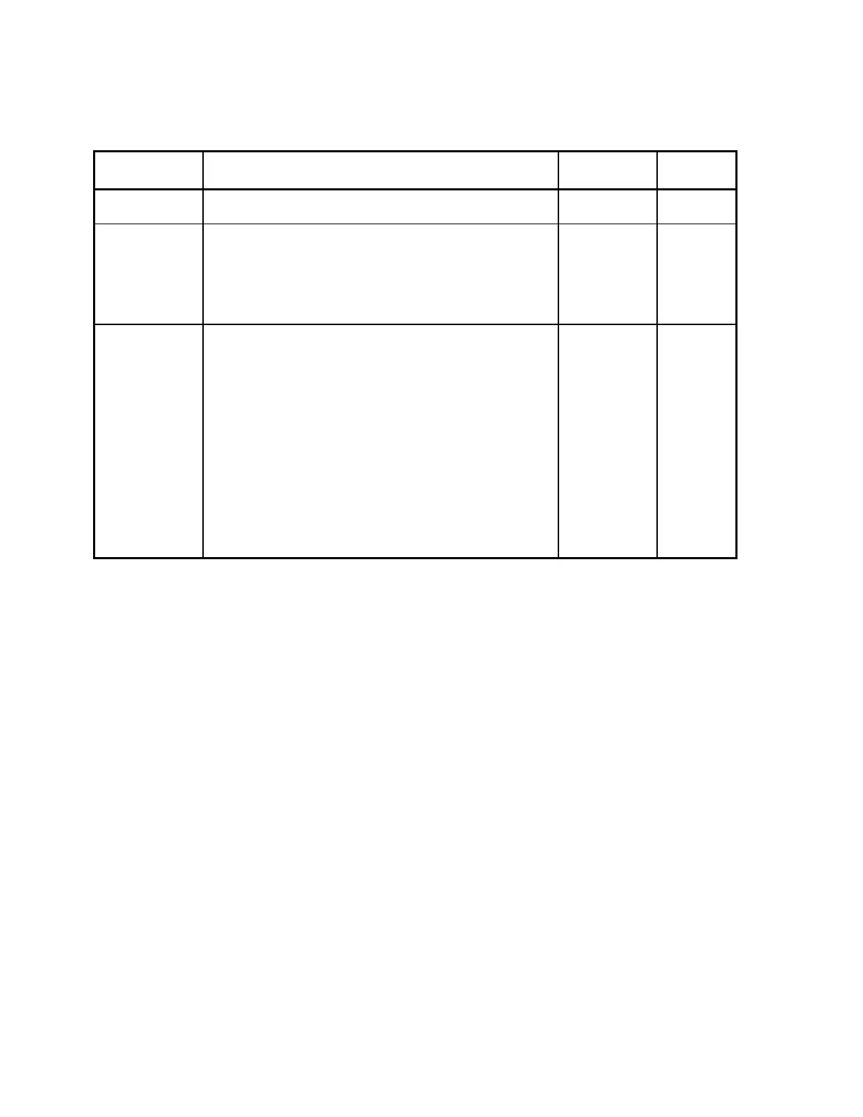
Table 2-21. Integrator/Multiplexor Board/Solid State Detector Boards
Interconnection Descriptions
Signal Description
I/M
Pins
SD
PINS
CHANNEL0 -
CHANNEL215
See Note 1 See Note 2
INTEGA
INTEGB
INTEGC
INTEGD
INTEGE
INTEGF
JP2-6, JP2-44
JP1-6, JP1-44
JP4-6, JP4-44
JP3-6, JP3-44
JP6-6, JP6-44
JP5-6, JP5-44
JP1-44, 6
JP2-44, 6
+15V
15V_RET
-15V
Powers the amplifiers and switches of the Solid State
Detector boards.
JP1-JP6-47,
JP1-JP6-48
JP1-JP6-3,
JP1-JP6-4,
JP1-JP6-5,
JP1-JP6-43,
JP1-JP6-45,
JP1-JP6-46,
JP1-JP6-49,
JP1-JP6-50
JP1-JP6-1,
JP1-JP6-2
JP1/2-47,
JP1/2-48
JP1/2-3,
JP1/2-4,
JP1/2-5,
JP1/2-43,
JP1/2-45,
P1/2-46,
JP1/2-49,
JP1/2-50
JP1/2-1,
JP1/2-2
Notes: 1. Refer to schematic drawing 140-0048-SD for connector and pin assignments (cannot scope these signals).
2. Refer to schematic drawing 140-0050-SD for connector and pin assignments (cannot scope these signals).
3. Note that the CHANNEL hardware numbers are reversed from the software numbers. e.g. Hardware
CHANNEL0 = software CHANNEL215.
INTEGRATOR/MULTIPLEXOR BOARD
The Integrator/Multiplexor receives up to 216 signals in parallel from the Solid State Detector
boards. The board integrates and stores those signals, and then applies the stored signals in four
groups of up to 64 signals in parallel to the Analog To Digital board.
Switched signals from the Solid State Detector board charge integrating capacitors on this board
during a given charging time. After the charging time, the switched signals are turned off and the
charges are held on the capacitors. Each integrator will be sampled by the multiplexor and sent
to the Analog To Digital board.. At the end of sampling, all the integrating capacitors will be
discharged in parallel by shorting them out with analog switches.
Each integrator has an additional input into which a test signal (TESTLVL) can be applied when
there are no X-rays present. This test signal is used to verify the operation of the integrators and
multiplexors.