Section 6 ROM
Rev. 7.00 Mar 10, 2005 page 170 of 652
REJ09B0042-0700
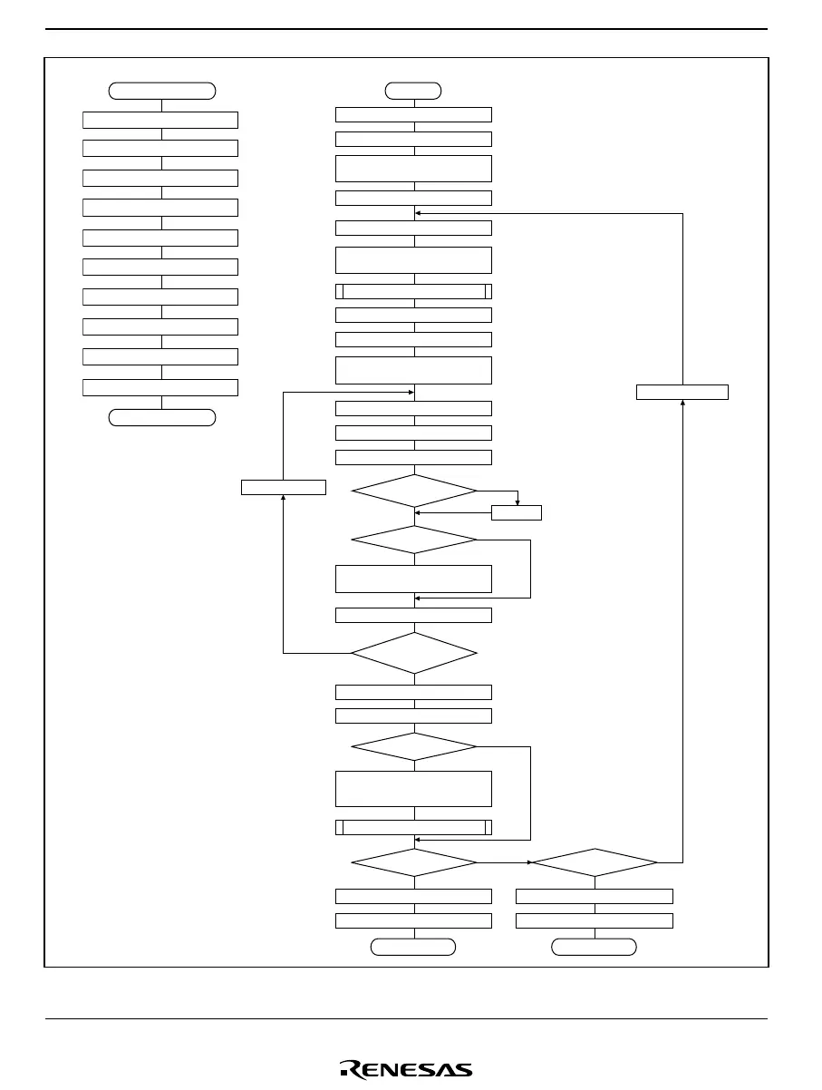
START
End of programming
Set SWE bit in FLMCR1
Write pulse application subroutine
Wait 1 µs
Apply Write Pulse
End Sub
Set PSU bit in FLMCR1
WDT enable
Disable WDT
Wait 50 µs
Set P bit in FLMCR1
Wait (Wait time = programming time)
Clear P bit in FLMCR1
Wait 5 µs
Clear PSU bit in FLMCR1
Wait 5 µs
n = 1
m = 0
No
No
No
Yes
Yes
Yes
Yes
Wait 4 µs
Wait 2 µs
Wait 2 µs
Apply Write pulse
Set PV bit in FLMCR1
H'FF dummy write to verify address
Read verify data
Reprogram data computation
Clear PV bit in FLMCR1
Clear SWE bit in FLMCR1
Increment address
Programming failure
Clear SWE bit in FLMCR1
Wait 100 µs
No
Yes
No
Yes
No
Wait 100 µs
n ≤ 1000 ?
Write 128-byte data in RAM reprogram
data area consecutively to flash memory
Store 128-byte program data in program
data area and reprogram data area
Apply Write Pulse
Sub-Routine-Call
Successively write 128-byte data from
additional-programming data area
in RAM to flash memory
Set block start address as
verify address
n ← n + 1
m = 1
m = 0 ?
n ≤ 6?
128-byte
data verification
completed?
n ≤ 6 ?
Additional-programming data
computation
Verify data =
write data?
Figure 6.10 Program/Program-Verify Flowchart

 Loading...


