Section 6 ROM
Rev. 7.00 Mar 10, 2005 page 180 of 652
REJ09B0042-0700
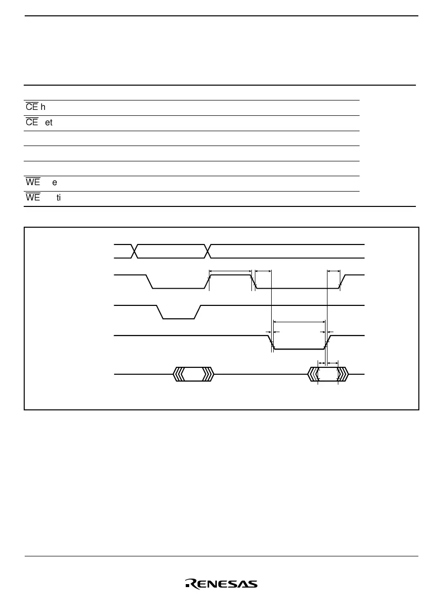
Table 6.15 AC Characteristics in Transition from Memory Read Mode to Another Mode
Conditions: V
CC
= 3.3 V ±0.3 V, V
SS
= 0 V, T
a
= 25°C ±5°C
Item Symbol Min Max Unit Notes
Command write cycle t
nxtc
20 — µs Figure 6.14
CE
hold time t
ceh
0—ns
CE
setup time t
ces
0—ns
Data hold time t
dh
50 — ns
Data setup time t
ds
50 — ns
Write pulse width t
wep
70 — ns
WE
rise time t
r
—30ns
WE
fall time t
f
—30ns
CE
A15−A0
OE
WE
I/O7−I/O0
Note: Do not enable WE and OE at the same time.
t
ceh
t
wep
t
f
t
r
t
ces
t
nxtc
Address stable
t
ds
t
dh
Other mode command writeMemory read mode
Figure 6.14 Timing Waveforms in Transition from Memory Read Mode to Another Mode

 Loading...


