Section 6 ROM
Rev. 7.00 Mar 10, 2005 page 181 of 652
REJ09B0042-0700
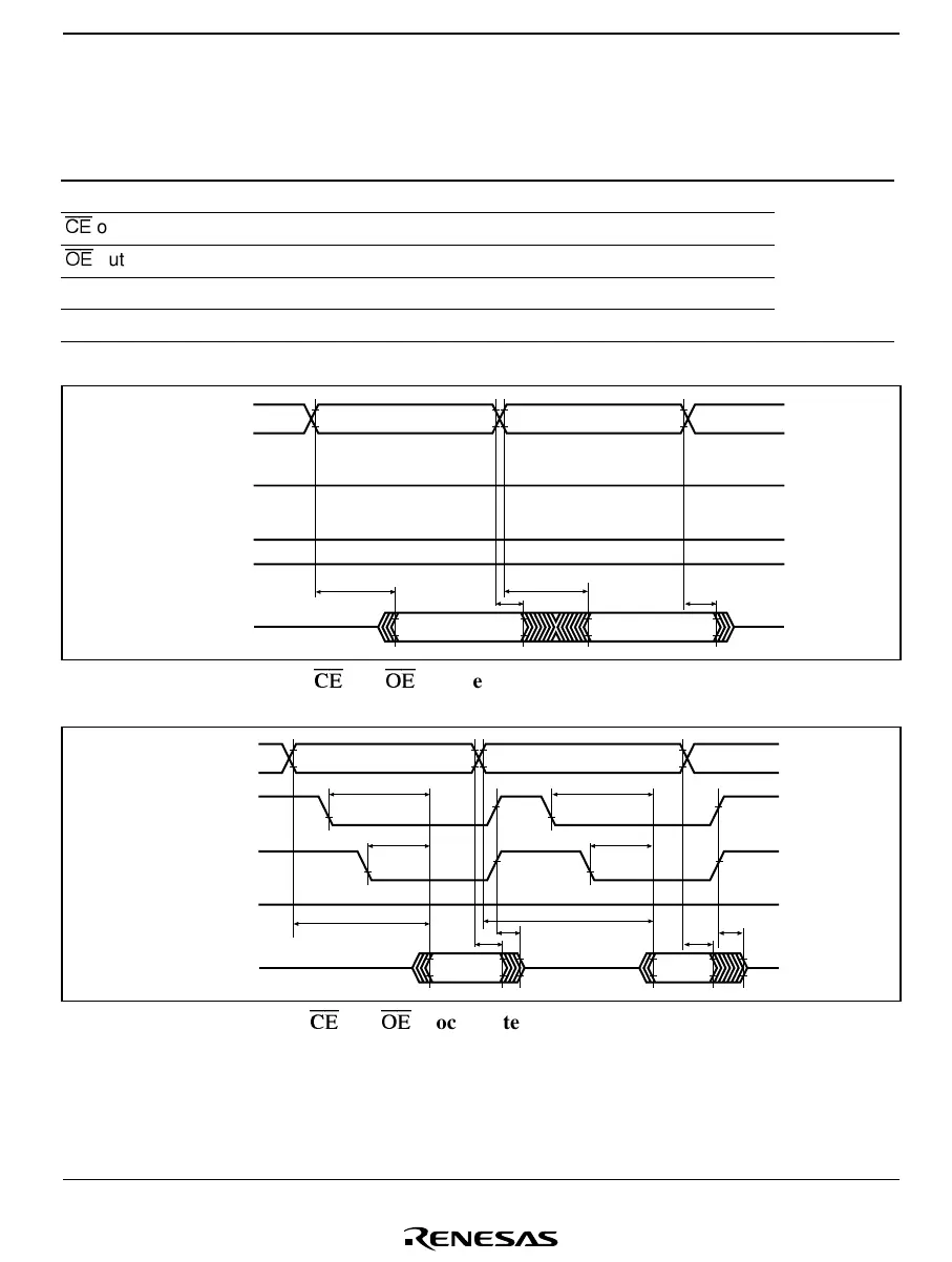
Table 6.16 AC Characteristics in Memory Read Mode
Conditions: V
CC
= 3.3 V ±0.3 V, V
SS
= 0 V, T
a
= 25°C ±5°C
Item Symbol Min Max Unit Notes
Access time t
acc
— 20 µs Figure 6.15
CE
output delay time t
ce
— 150 ns Figure 6.16
OE
output delay time t
oe
— 150 ns
Output disable delay time t
df
— 100 ns
Data output hold time t
oh
5—ns
CE
A15−A0
OE
WE
I/O7−I/O0
t
acc
t
acc
t
oh
t
oh
Address stableAddress stable
Figure 6.15
CE
and
OE
Enable State Read Timing Waveforms
CE
A15−A0
OE
WE
I/O7−I/O0
t
acc
t
ce
t
oe
t
oe
t
ce
t
acc
t
oh
t
df
t
df
t
oh
Address stableAddress stable
Figure 6.16
CE
and
OE
Clock System Read Timing Waveforms

 Loading...


