Section 9 Timers
Rev. 7.00 Mar 10, 2005 page 327 of 652
REJ09B0042-0700
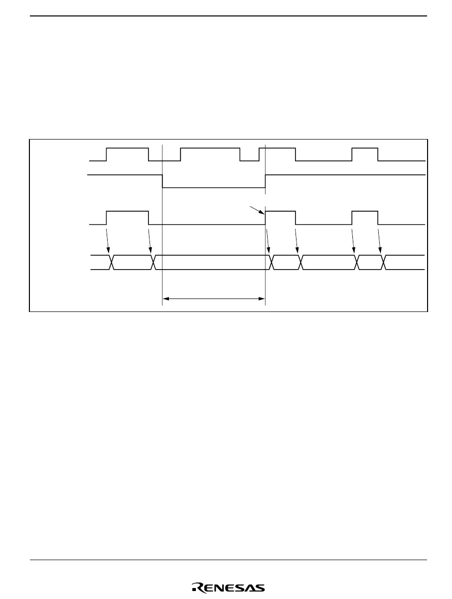
Clock Input Enable/Disable Function Operation
The clock input to the event counter can be controlled by the IRQAEC pin when ECPWME in
AEGSR is 0, and by event counter PWM output IECPWM when ECPWME in AEGSR is 1. As
this function forcibly terminates the clock input by each signal, a maximum error of one count will
occur depending the IRQAEC or IECPWM timing.
Figure 9.23 shows an example of the operation of this function.
Clock stopped
N+2 N+3 N+4 N+5 N+6N N+1
Edge generated by clock return
Input event
IRQAEC or
IECPWM
ctually counted
clock source
Counter value
Figure 9.23 Example of Clock Control Operation

 Loading...


