Section 1 Overview
Rev. 7.00 Mar 10, 2005 page 13 of 652
REJ09B0042-0700
Y
X
(0, 0)
61
59
57
55
53
51
49
47
45
43
60
58
56
54
52
50
48
46
44
42
81 79 77 75 73 71 69 67 65 63
1
3
5
7
9
11
13
15
17
19
21
2
4
6
8
10
12
14
16
18
20
22
23
80 78 76 74 72 70 68 66 64 62
25 27 29 31 33 35 37 39 41
24 26 28 30 32 34 36 38 40
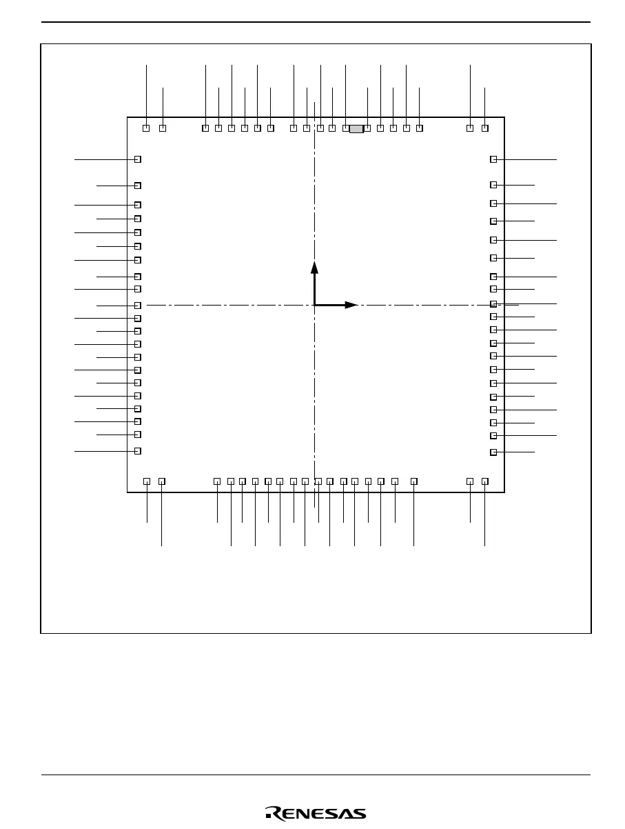
Chip size: 3.99 mm × 3.99 mm
Voltage level on the back of the chip: GND
Type code
Figure 1.5 Bonding Pad Location Diagram of HCD64338024, HCD64338023,
HCD64338022, HCD64338021, and HCD64338020 (Top View)

 Loading...


