Section 1 Overview
Rev. 7.00 Mar 10, 2005 page 14 of 652
REJ09B0042-0700
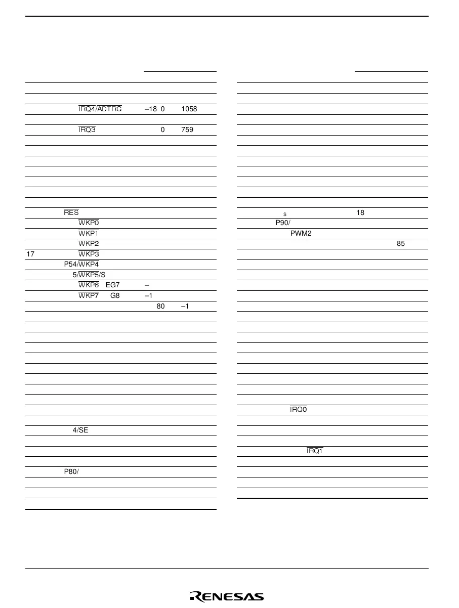
Table 1.2 Bonding Pad Coordinates of HCD64338024, HCD64338023, HCD64338022,
HCD64338021, and HCD64338020
Coordinates Coordinates
Pad No. Pad Name X (µ
µµ
µm) Y (µ
µµ
µm) Pad No. Pad Name X (µ
µµ
µm) Y (µ
µµ
µm)
1AV
CC
–1870 1546 42 P84/SEG29 1870 –1571
2 P13/TMIG –1870 1274 43 P85/SEG30 1870 –1395
3 P14/
IRQ4
/
ADTRG
–1870 1058 44 P86/SEG31 1870 –1251
4 P16 –1870 909 45 P87/SEG32 1870 –1111
5 P17/
IRQ3
/TMIF –1870 759 46 PA3/COM4 1870 –970
6 X1 –1870 608 47 PA2/COM3 1870 –831
7 X2 –1870 475 48 PA1/COM2 1870 –691
8AV
SS
–1870 304 49 PA0/COM1 1870 –550
9V
SS
–1870 173 50 V3 1870 –410
10 OSC2 –1870 –10 51 V2 1870 –270
11 OSC1 –1870 –150 52 V1 1870 –131
12 TEST –1870 –290 53 V
CC
1870 10
13
RES
–1870 –425 54 V
SS
1870 150
14 P50/
WKP0
/SEG1 –1870 –560 55 P90/PWM1 1870 293
15 P51/
WKP1
/SEG2 –1870 –695 56 P91/PWM2 1870 489
16 P52/
WKP2
/SEG3 –1870 –831 57 P92 1870 685
17 P53/
WKP3
/SEG4 –1870 –966 58 P93 1870 880
18 P54/
WKP4
/SEG5 –1870 –1101 59 P94 1870 1076
19 P55/
WKP5
/SEG6 –1870 –1236 60 P95 1870 1274
20 P56/
WKP6
/SEG7 –1870 –1379 61 IRQAEC 1870 1546
21 P57/
WKP7
/SEG8 –1870 –1561 62 P30/UD 1782 1872
22 P60/SEG9 –1780 –1872 63 P31/TMOFL 1621 1872
23 P61/SEG10 –1621 –1872 64 P32/TMOFH 1084 1872
24 P62/SEG11 –1037 –1872 65 P33 948 1872
25 P63/SEG12 –896 –1872 66 P34 810 1872
26 P64/SEG13 –765 –1872 67 P35 673 1872
27 P65/SEG14 –635 –1872 68 P36/AEVH 536 1872
28 P66/SEG15 –502 –1872 69 P37/AEVL 311 1872
29 P67/SEG16 –371 –1872 70 P40/SCK32 176 1872
30 P70/SEG17 –239 –1872 71 P41/RXD32 38 1872
31 P71/SEG18 –108 –1872 72 P42/TXD32 –99 1872
32 P72/SEG19 23 –1872 73 P43/
IRQ0
–234 1872
33 P73/SEG20 156 –1872 74 PB0/AN0 –482 1872
34 P74/SEG21 287 –1872 75 PB1/AN1 –614 1872
35 P75/SEG22 419 –1872 76 PB2/AN2 –745 1872
36 P76/SEG23 550 –1872 77 PB3/AN3/
IRQ1
/TMIC –878 1872
37 P77/SEG24 682 –1872 78 PB4/AN4 –1008 1872
38 P80/SEG25 833 –1872 79 PB5/AN5 –1148 1872
39 P81/SEG26 1040 –1872 80 PB6/AN6 –1621 1872
40 P82/SEG27 1621 –1872 81 PB7/AN7 –1782 1872
41 P83/SEG28 1782 –1872
Note: V
SS
Pads (No. 8 and 9) should be connected to power supply lines.
TEST Pad (No. 12) should be connected to V
SS
.
If the pad of these aren’t connected to the power supply line, the LSI will not operate correctly. These values show the
coordinates of the centers of pads. The accuracy is ±5 µm. The home-point position is the chip’s center and the center
is located at half the distance between the upper and lower pads and left and right pads.
 Loading...


