Section 1 Overview
Rev. 7.00 Mar 10, 2005 page 24 of 652
REJ09B0042-0700
Pin No.
Type Symbol
FP-80A
TFP-80C
FP-80B TLP-85V
Pad
No.
*
1
Pad
No.
*
2
Pad
No.
*
3
I/O Name and Functions
A/D
converter
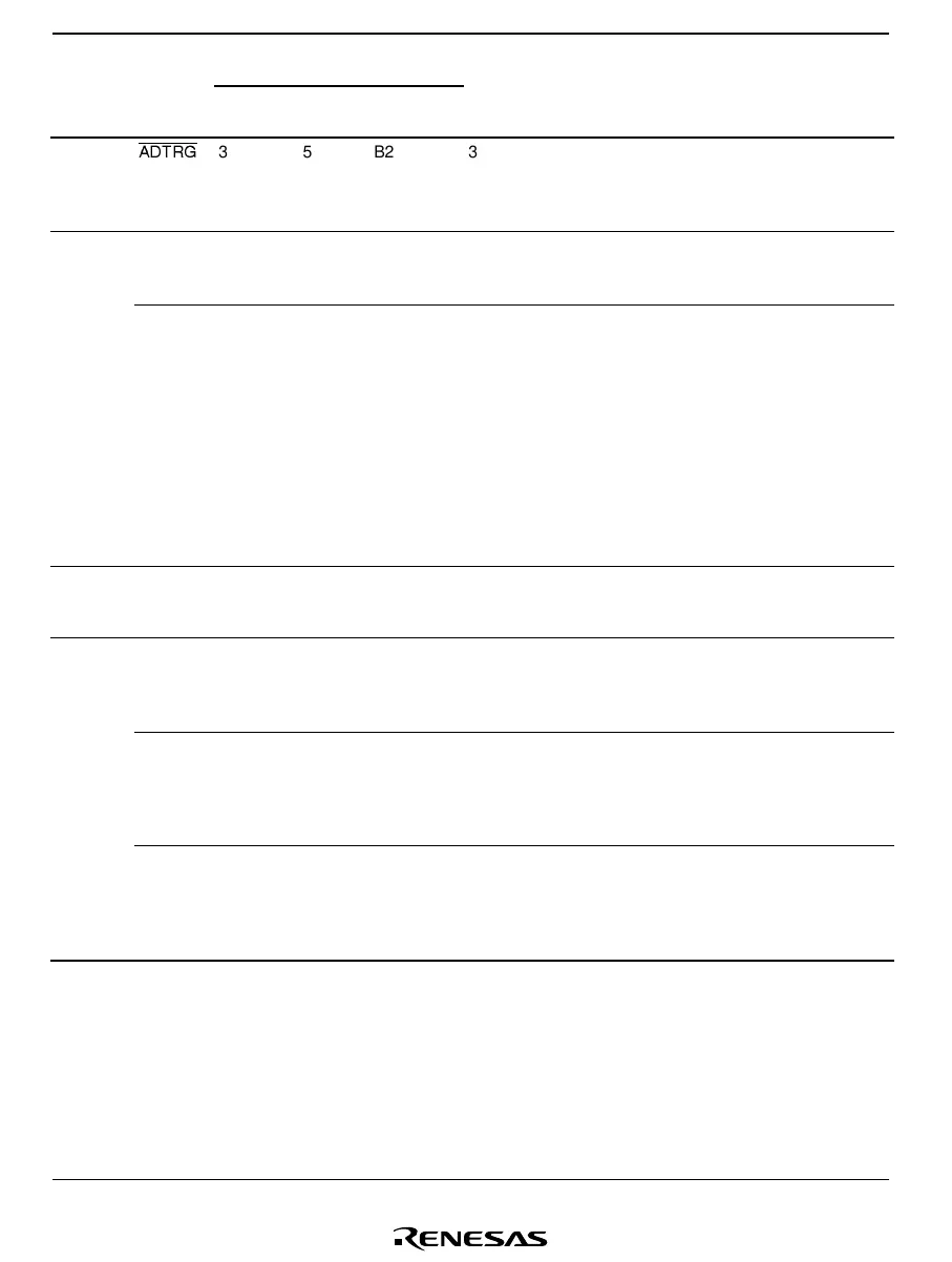
ADTRG
3 5 B2 343Input
A/D converter trigger
input: This is the external
trigger input pin to the A/D
converter.
LCD
controller/
driver
COM
4
to
COM
1
45 to 48 47 to 50
G10, G8
G9, F10
46 to
49
47 to
50
45 to
48
Output
LCD common output:
These are the LCD
common output pins.
SEG
32
to
SEG
1
44 to 13 46 to 15 H9, J9,
H10, J10,
K8, K9, H8,
K7, J8, J7,
K6, H7, H6,
J5, J6, H5,
K5, J4, H4,
K4, J3, J2,
K3, K2, H1,
J1, H3, G1,
H2, G2, F1,
G3
45 to
14
46 to
15
44 to
13
Output LCD segment output:
These are the LCD
segment output pins.
NC NC — — A1, A10,
D4, K2,
K10
———— NC pin
V
ref
57 — — ———Input
LVD reference voltage
input: This is the LVD
reference voltage input
pin.
Low-
voltage
detect
circuit
(LVD)
*
4
extD 73 — — — — — Input
LVD power supply drop
detect voltage input:
This is the LVD power
supply drop detect
voltage input pin.
extD 74 — — — — — Input
LVD power supply rise
detect voltage input:
This is the LVD power
supply rise detect voltage
input pin.
Notes: 1. Pad number for HCD64338024, HCD64338023, HCD64338022, HCD64338021, and
HCD64338020.
2. Pad number for HCD64F38024 and HCD64F38024R.
3. Pad number for HCD64338024S, HCD64338023S, HCD64338022S, HCD64338021S,
and HCD64338020S.
4. H8/38124 Group only
5. Does not apply to H8/38124 Group.

 Loading...


