Lesson 1 – Analog Modules
79
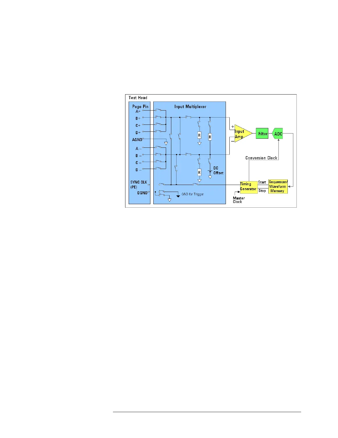
High Resolution / High Speed Digitizer
The following figure shows the block diagram of the high
resolution digitizer and high speed digitizer:
Block Diagram of WDA/WDB
The waveform digitizer consists of the following blocks:
1 Input Multiplexer
For A+, A-, B+, B-, C+, C-, D+, and D- input pins, the input
multiplexer is used to specify one of 8 single-ended inputs or one
of 4 differential inputs. The allowable pin combinations for the
differential inputs are A+/A-, B+/B-, C+/C-, and D+/D-.
In addition, the multiplexer can make the following routes for
these pins and SYNC_CLK pin:
• DC routes to perform DC measurement at one of the input pins via
the SYNC CLK pin.
• Loop back routes from one digitizer pin to another.
For details about these routes, see “Pin Connections with an
Analog Module’s Multiplexer” on page 99.
NOTE The SYNC CLK pin is also called the trigger pin. For the WDB, there
is SYNC DATA pin, which is not shown in the above figure.
SYNC_DATA is currently not used.
2 Input Routes
For measuring a single-ended signal, the signal is fed to one of the
pogo pins. The input multiplexer connects the pogo pin and input
amplifier by closing the internal relays between them.
 Loading...