Tightly-Coupled Memory Interface
5-10 Copyright © 2001-2003 ARM Limited. All rights reserved. ARM DDI0198D
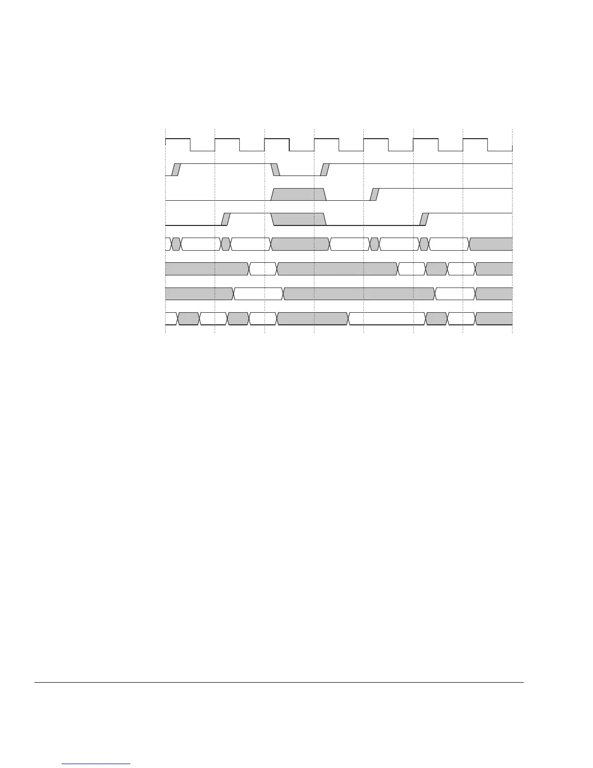
Figure 5-3 Data side zero wait state accesses
In cycle T1, a nonsequential read request is made to address A.
In cycle T2, a nonsequential word write request is made to address B and data is
returned for the access to A.
In cycle T3, no request is made.
In cycle T4, a nonsequential read request is made to address C.
In cycle T5, a sequential read request is made to address C+1 and data is returned for
the access to C.
In cycle T6, a nonsequential byte write request is made to address D.
5.3.2 DMA access to zero wait state TCM
For DMA accesses to zero wait state memories, the TCM DMA interface can be used
which enables an alternative source of address and chip-select to be passed through to
the TCM memories without impacting timing. Figure 5-4 on page 5-11 shows the
relationship between DRDMAEN, DRDMACS, DRDMAADDR, DRADDR and
DRCS.
CLK
DRCS
DRSEQ
DRADDR A B C C+1 D
DRRD D(A) D(C)
D(C+1)
T1 T2 T3 T4 T5 T6 T7
DnRW
DRWD D(B) D(D)
DRWBL 0000 1111 0000 0001

 Loading...

