Programmer’s Model
2-12 Copyright © 2001-2003 ARM Limited. All rights reserved. ARM DDI0198D
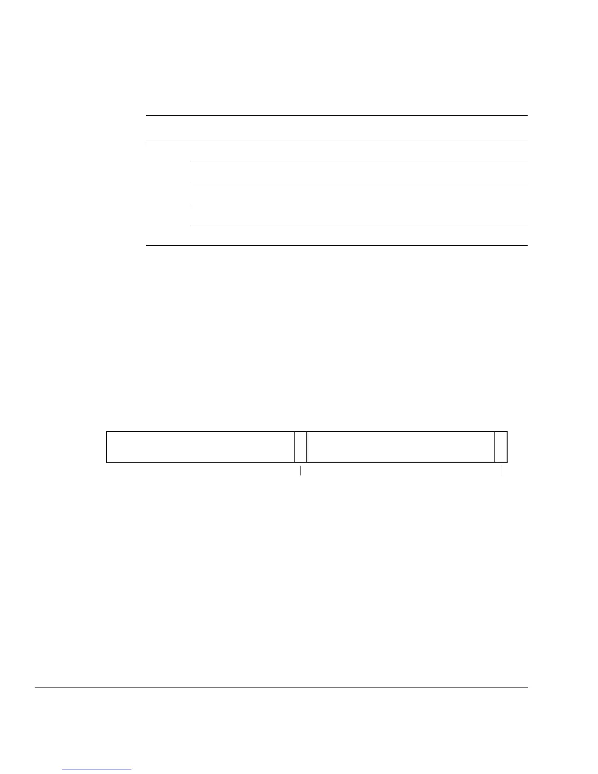
TCM Status Register c0
This is a read-only register that enables operating systems to establish if TCM memories
are present. See also TCM Region Register c9 on page 2-29.
You can access the TCM Status Register by reading CP15 register c0 with the Opcode_2
field set to 2. For example:
MRC p15,0,<Rd>,c0,c0,2 ;returns TCM details
The format of the TCM Status Register is shown in Figure 2-4.
Figure 2-4 TCM Status Register format
2.3.2 Control Register c1
Register c1 is the Control Register for the ARM926EJ-S processor. This register
specifies the configuration used to enable and disable the caches and MMU. It is
recommended that you access this register using a read-modify-write sequence.
For both reading and writing, the CRm and Opcode_2 fields Should Be Zero. To read
and write this register, use the instructions:
MRC p15, 0, <Rd>, c1, c0, 0 ; read control register
Isize Reserved [11:10] b00
Size [9:6] b0101 = 16KB
Assoc [5:3] b010 = 4-way
M[2] b0
Len [1:0] b10 = 8 words per line (32 bytes)
Table 2-10 Example Cache Type Register format (continued)
Function Register bits Value
ITCM
present
SBZ/UNP
31 17 16 15 1 0
DTCM
present
SBZ/UNP