Tightly-Coupled Memory Interface
ARM DDI0198D Copyright © 2001-2003 ARM Limited. All rights reserved. 5-17
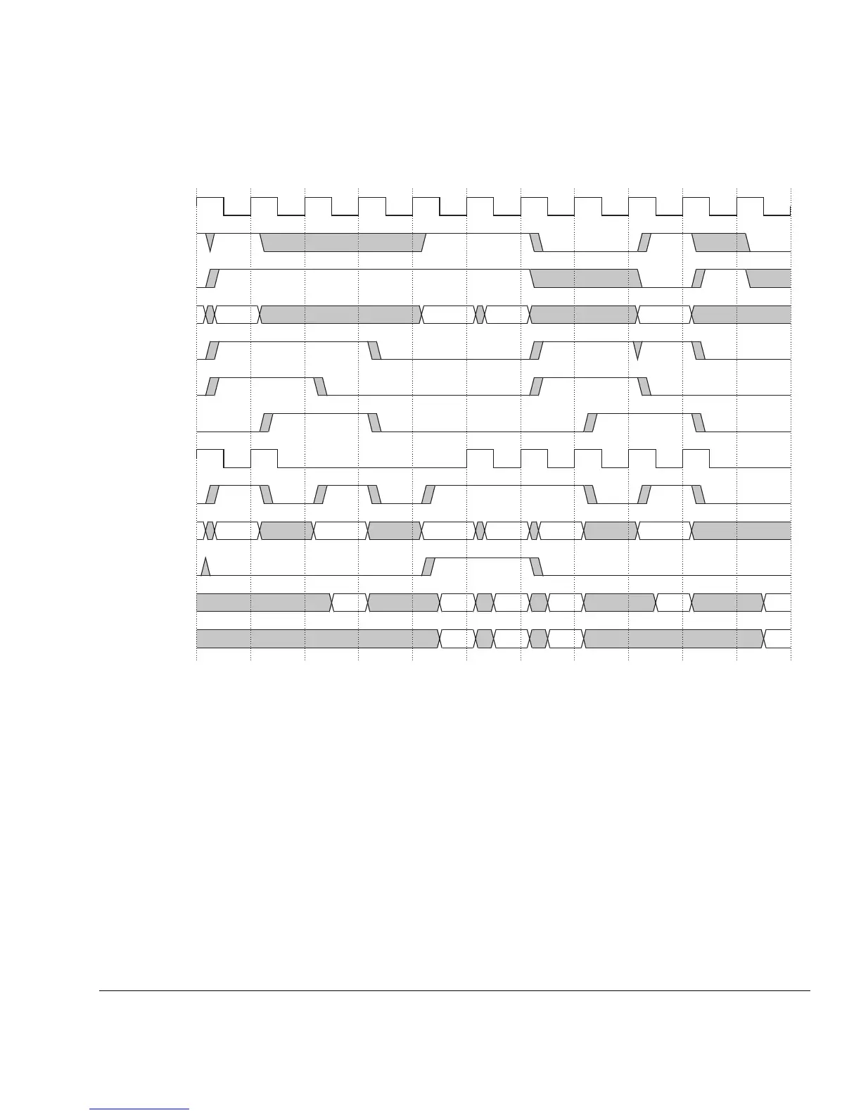
Figure 5-11 Cycle timing of circuit with DMA and single wait state for nonsequential accesses
In cycle T1, the ARM926EJ-S initiates a sequential request to address A and the DMA
gains ownership of the TCM. DRWAIT is asserted because of DMAWAIT. The CS, A,
WE signals for the TCM are sourced from the DMA. The values of DRADDR,
DRBWL and DnRW are registered.
In cycle T2, the DMA access is still active (two cycle nonsequential access). DRWAIT
is held HIGH because of DMAWAIT.
In cycle T3, the DMA access completes and DMAWAIT is deasserted. The access
attributes captured at the end of T1 are used to generate the CS, A and WE signals for
the TCM. DRWAIT is asserted because of FORCE_NSEQ.
In cycle T4, FORCE_NSEQ is deasserted causing DRWAIT to be deasserted
indicating that the access will complete in the next cycle.
T1 T2 T3 T4 T5 T6 T7 T8 T9 T10 T11
CLK
DRCS
DRSEQ
DRADDR
DRWAIT
DMAWAIT
FORCE_NSEQ
REQCLK
CS
A
SEQ
RD
DRRD
A A+1 A+2 D
B A+1 A+2 DA C
D(B) D(A)
D(A+1) D(A+2)
D(C)
D(D)
D(A)
D(A+1) D(A+2) D(D)

 Loading...

