CP15 Test and Debug Registers
ARM DDI0198D Copyright © 2001-2003 ARM Limited. All rights reserved. B-7
2. Use the following MMU test operation instructions to access the MVA tag:
MRC p15, 4/5, <Rd>, c15, c2, 0 ; read tag in main TLB
MCR p15, 4/5, <Rd>, c15, c3, 0 ; write tag in main TLB
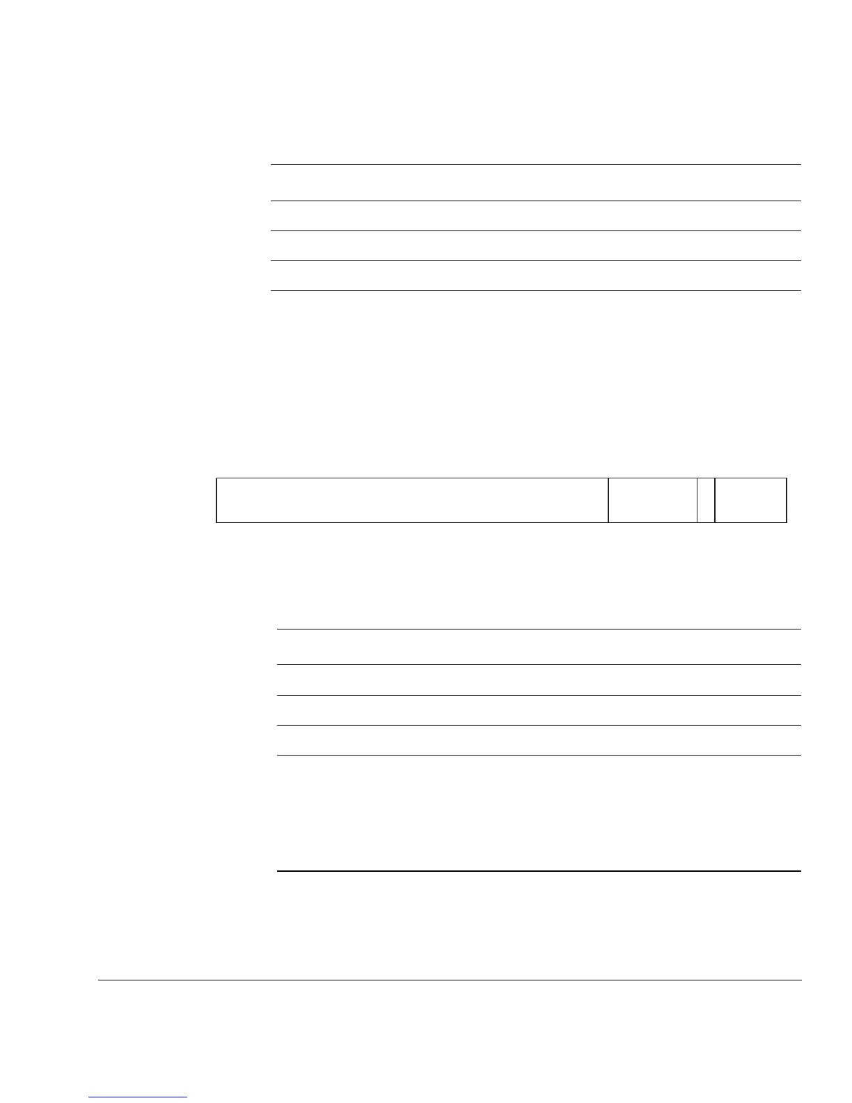
The Rd register contains the read or write data as Figure B-3 shows.
Figure B-3 Rd format for accessing MVA tag of main or lockdown TLB entry
Table B-5 describes the MVA tag access bit fields in the Rd register.
3. Use the following MMU Test Register instructions to access the PA and access
permission data:
MRC p15, 4/5, <Rd>, c15, c4, 0 ; read PA and access permission data
[30:15] - Should Be Zero.
[14:10] Indexed entry Indexed entry in main TLB.
[9:0] - Should Be Zero.
Table B-4 Encoding of the main TLB entry-select bit fields
Bit Name Definition
0
MVA tag
SBZ
43951031
V
Size of
entry
Table B-5 Encoding of the TLB MVA tag bit fields
Bit Name Definition
[31:10] MVA tag Modified virtual address.
[9:5] - Should Be Zero.
[4] V Valid bit.
[3:0] Size of entry Size of entry:
b1011 = 1MB section
b0111 = 64KB page
b0101 = 16KB subpage of 64KB page
b0011 = 4KB page
b0001 = 1KB page or 1KB subpage of 4KB page.

 Loading...

