Tightly-Coupled Memory Interface
ARM DDI0198D Copyright © 2001-2003 ARM Limited. All rights reserved. 5-21
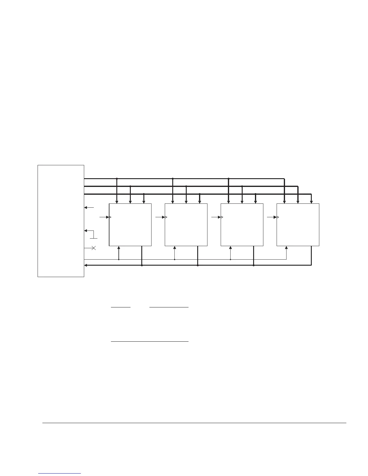
The rules for connecting four RAM blocks are:
• Each byte-wide RAM has the same address and chip-select control as the
word-wide RAM.
• The following connections must be made:
— DRWBL[0], DRWD[7:0], and DRRD[7:0], connect to RAM byte 0
— DRWBL[1], DRWD[15:8], and DRRD[15:8], connect to RAM byte 1
— DRWBL[2], DRWD[23:16], and DRRD[23:16], connect to RAM byte 2
— DRWBL[3], DRWD[31:24], and DRRD[31:24], connect to RAM byte 3.
Figure 5-13 Byte-banks of RAM example
Note
In little-endian mode, DRWBL[0] indicates the LSB of the word and DRWBL[3]
indicates the MSB. In big-endian mode, DRWBL[3] indicates the LSB of the word and
DRWBL[0] indicates the MSB.
5.5.3 Multiple banks of RAM example
If you have to create a large memory out of smaller RAM blocks, there are two methods
for doing this:
• If minimizing power consumption is more important than a fast design, you must
follow the example in Optimizing for power on page 5-22.
32K RAM
b0110
DIN[7:0] WE
DRWR[7:0]
A[14:0]
DRADDR[14:0]
DRWBL[0]
DRWR[15:8]
DRWBL[1]
DOUT[7:0]CS
DRWR[23:16]
DRWBL[2]
DRWR[31:24]
DRWBL[3]
DRRD[7:0] DRRD[15:8] DRRD[23:16] DRRD[31:24]
CLK
ARM926EJ-S
DRWD[31:0]
DRADDR[17:0]
DRSIZE[3:0]
DRWAIT
DRRD[31:0]
DRWBL[3:0]
DRCS
32K RAM
DIN[7:0] WEA[14:0]
DOUT[7:0]CS
CLK
32K RAM
DIN[7:0] WEA[14:0]
DOUT[7:0]CS
CLK
32K RAM
DIN[7:0] WEA[14:0]
DOUT[7:0]CS
CLK
CLK
Byte 0 Byte 1 Byte 2 Byte 3
DRnRW