Tightly-Coupled Memory Interface
ARM DDI0198D Copyright © 2001-2003 ARM Limited. All rights reserved. 5-23
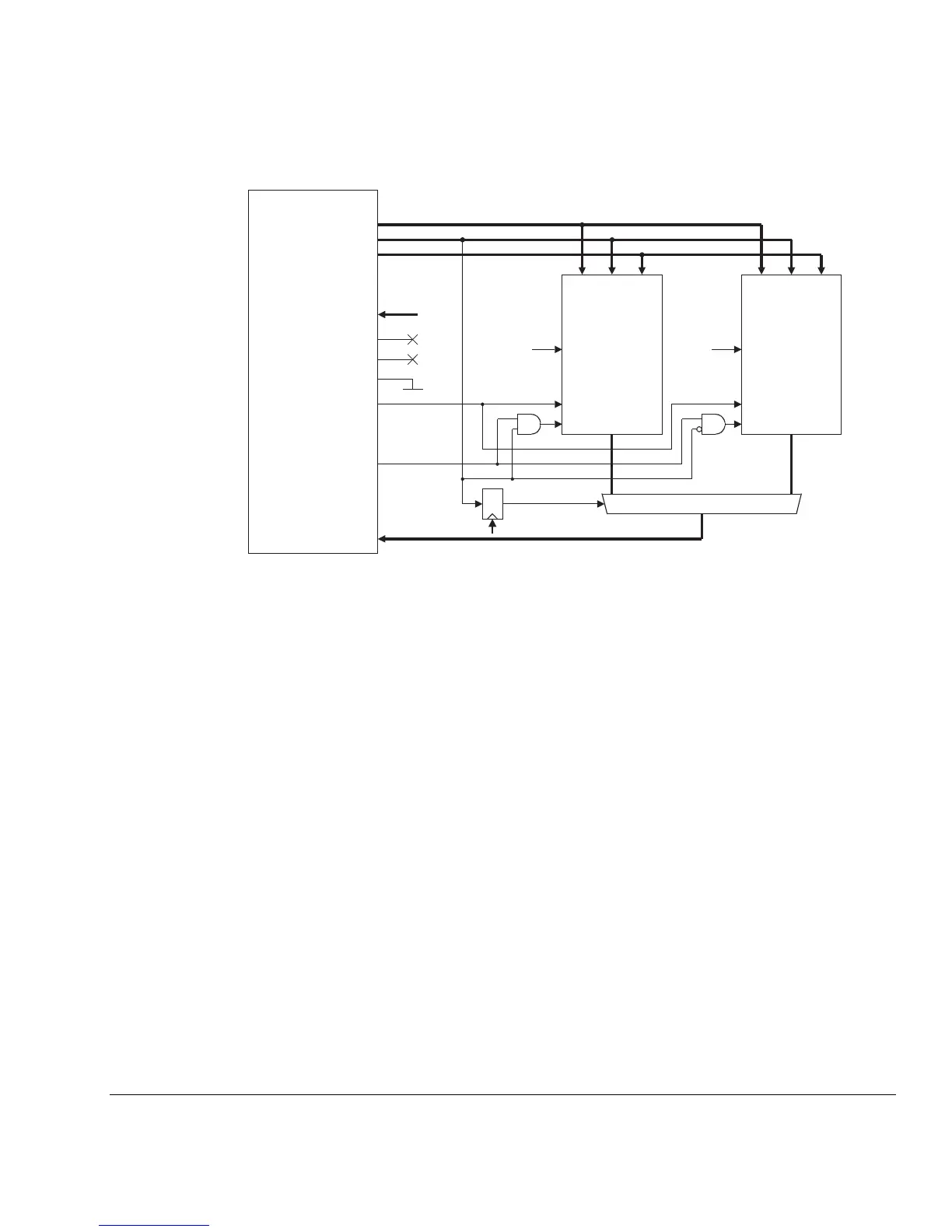
Figure 5-14 Optimizing for power
Optimizing for speed
Figure 5-15 on page 5-24 shows how to produce a large memory from two smaller
RAM blocks if you are optimizing for speed. Separate write enable control is required
for each RAM block:
WE_bank0 = ~DRADDR[14] & DRnRW
WE_bank1 = DRADDR[14] & DRnRW
No logic is added to the critical DRCS path, but both RAMs are enabled whenever
DRCS is asserted, resulting in higher power consumption.
DRSIZE[3:0]
DRIDLE
DRCS
DRSEQ
DRWAIT
ARM926EJ-S
RAM 64KB
CLK
CS DOUT[31:0]
RAM 64KB
CLK
CS DOUT[31:0]
b1000
DRADDR[14]
DRRD[31:0]
DRADDR[13:0]
DRWD[31:0]
DRADDR[17:0]
DRWBL[3:0]
DRADDR[13:0]
CLK
DIN[31:0] BW[3:0]
A[13:0]
DIN[31:0] BW[3:0]
A[13:0]
Bank 1 Bank 0
WEDRnRW WE

 Loading...

