CP15 Test and Debug Registers
B-2 Copyright © 2001-2003 ARM Limited. All rights reserved. ARM DDI0198D
B.1 About the Test and Debug Registers
The ARM926EJ-S Test and Debug Registers, CP15 c15, provide additional
device-specific test operations. You can use the registers to access and control the
following:
• Debug Override Register
• Debug and Test Address Register on page B-4
• Trace Control Register on page B-5
• MMU test operations on page B-5
• Cache Debug Control Register on page B-12
• MMU Debug Control Register on page B-13
• Memory Region Remap Register on page B-15.
You must only use these operations for test. The ARM Architecture Reference Manual
describes this register as implementation-defined.
The format of the CP15 test and debug operations is:
MCR/MRC p15, <Opcode_1>, <Rd>, c15, <CRm>, <Opcode_2>
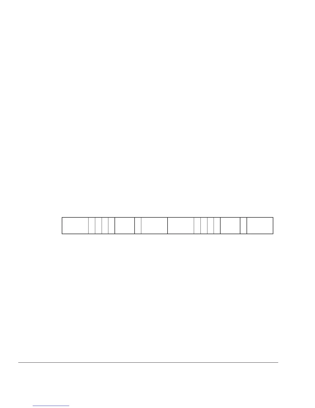
The MRC and MCR bit pattern is shown in Figure B-1.
Figure B-1 CP15 MRC and MCR bit pattern
The L bit distinguishes between an MCR (L = 1) and an MRC (L = 0).
B.1.1 Debug Override Register
You can use the Debug Override Register to modify the behavior of the ARM926EJ-S
core from the default behavior.
The function of each ARM926EJ-S Debug Override Register bit is shown in Table B-1
on page B-3.
The Debug Override Register can be accessed by using the following instructions:
MRC{cond} p15,0,<Rd>,c15,c0,0 ; Read Debug Override Register
MCR{cond} p15,0,<Rd>,c15,c0,0 ; Write Debug Override Register
Cond
31 28 27 26 25 24 23 21 20 19 16 15 12 11 10 9 8 7 5 4 3 0
1 1 1 0
Opcode
_1
L CRn Rd 1 1 1 1
Opcode
_2
1 CRm

 Loading...

