Bus Interface Unit
6-10 Copyright © 2001-2003 ARM Limited. All rights reserved. ARM DDI0198D
6.2.6 AHB clocking
The ARM926EJ-S design uses a single clock, CLK. To run the ARM926EJ-S processor
at a higher frequency than the AHB system bus, a separate AHB clock enable for each
of the two bus masters is required (in a multi-AHB system each AHB system can be
running at a different frequency):
DHCLKEN Is used to signify the rising edge of HCLK for the system data
BIU bus master.
IHCLKEN Is used to signify the rising edge of HCLK for the system
instruction BIU bus master.
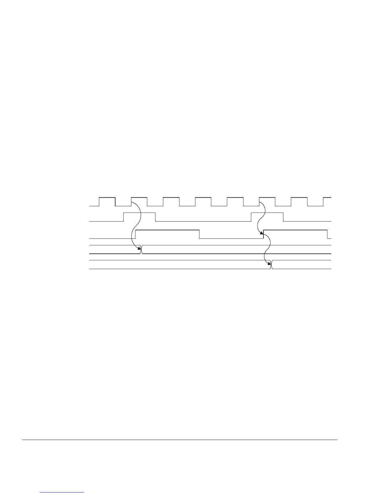
Figure 6-3 shows the relationships between CLK, HCLK, DHCLKEN, and
IHCLKEN.
Figure 6-3 AHB clock relationships
For single and multi-layer AHB systems, DHCLKEN and IHCLKEN must be tied
together. If HCLK and CLK are the same frequency, the relevant HCLKEN input (or
inputs) must be tied HIGH.
CLK and HCLK must be synchronous. The skew between CLK and HCLK must be
minimized.
6.2.7 External Abort limitations
Only certain types of accesses cause an External Abort if an Error response is returned
for an AHB transfer. These are:
• page table walk
• noncached read
• nonbuffered write
• noncached read-lock-write (SWP).
CLK
D/IHCLKEN
HCLK
AHB outputs
from ARM926EJ-S
Skew between CLK and HCLK
AHB inputs
to ARM926EJ-S

 Loading...

