CP15 Test and Debug Registers
ARM DDI0198D Copyright © 2001-2003 ARM Limited. All rights reserved. B-15
B.1.7 Memory Region Remap Register
The read/write Memory Region Remap Register overrides the setting specified in the
MMU page tables, and the default behavior if the MMU is disabled.
The Memory Region Register has four fields for remapping instruction-side memory
regions and four fields for remapping data-side memory regions.
You can access the Memory Region Remap Register with the instructions in
Table B-11.
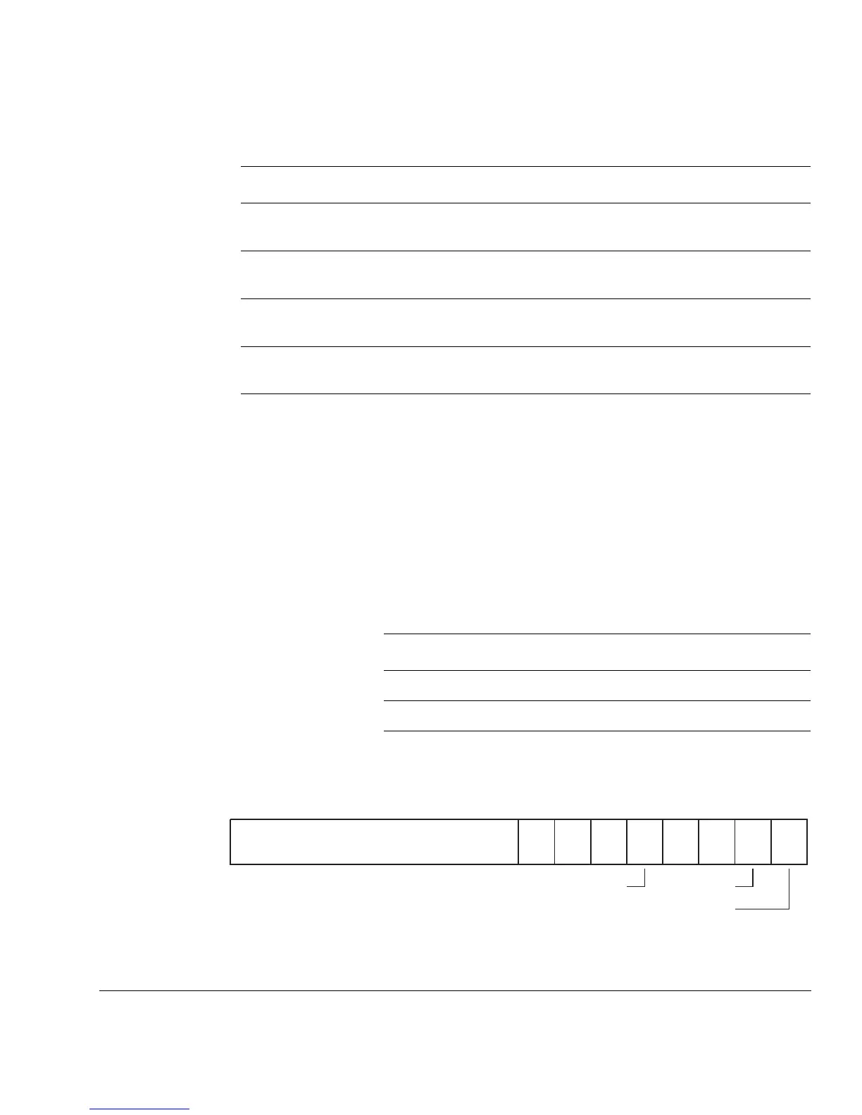
Figure B-9 shows the bit fields of the Memory Region Remap Register.
Figure B-9 Memory Region Remap Register format
[3] DIUTM Disable instruction micro TLB match 0 = Enable I-micro TLB load
1 = Disable I-micro TLB load
[2] DDUTM Disable data micro TLB match 0 = Enable D-micro TLB match
1 = Disable D-micro TLB match
[1] DIUTL Disable instruction micro TLB load 0 = Enable D-micro TLB load
1 = Disable D-micro TLB load
[0] DDUTL Disable data micro TLB load 0 = Enable I-micro TLB load
1 = Disable I-micro TLB load
Table B-10 MMU Debug Control Register bit assignments (continued)
Bit Name Function Description
Table B-11 Memory Region Remap Register instructions
Instruction Operation
MRC p15, 0, Rd, c15, c2, 0
Read Memory Region Remap Register
MCR p15, 0, Rd, c15, c2, 0
Write Memory Region Remap Register
15 12 11 8 7 4 3 0
SBZ
1314 910
DNCB
56
12
DNCNB
DWTDWB
INCNB
INCBIWTIWB
31 16

 Loading...

