CP15 Test and Debug Registers
B-8 Copyright © 2001-2003 ARM Limited. All rights reserved. ARM DDI0198D
MCR p15, 4/5, <Rd>, c15, c5, 0 ; write PA and access permission data
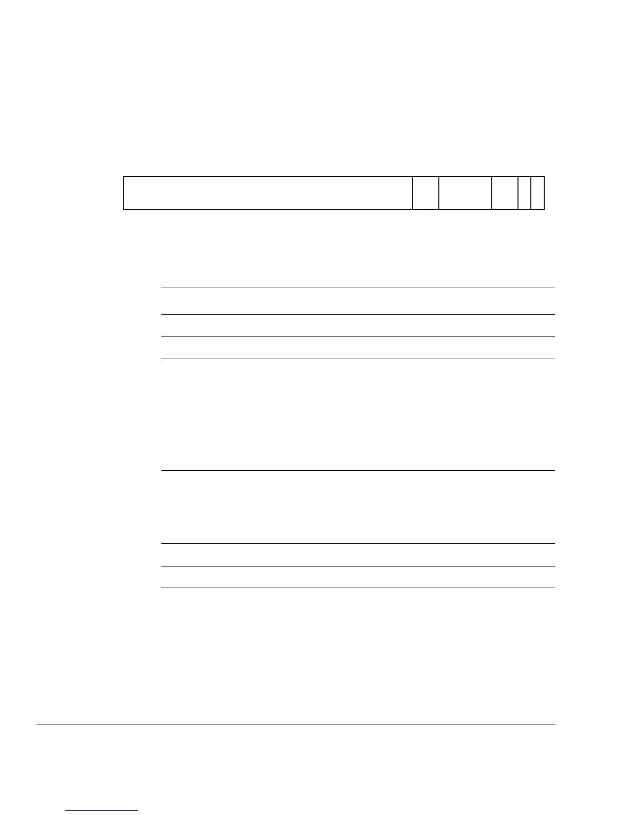
The Rd register contains the read or write data as shown in Figure B-4.
Figure B-4 Rd format for accessing PA and AP data of main or lockdown TLB entry
Table B-6 describes the PA and access permission bit fields in the Rd register.
4. Use the following instruction to complete a write to an entry:
MCR p15, 4/5, Rd, c15, c7, 0 ; transfer main storage into RAM
To write an entry into the 2-way main TLB, the full sequence is therefore:
MCR p15, 4/5, <Rd>, c15, c3, 0 ; write tag main TLB storage reg
MCR p15, 4/5, <Rd>, c15, c5, 0 ; write PA/PROT main TLB storage reg
MCR p15, 4/5, <Rd>, c15, c7, 0 ; transfer main storage into RAM
43 0
PA
9
Domain
select
SBZ
12
C
AP
[1:0]
B
31 10
78
Table B-6 Encoding of the TLB entry PA and AP bit fields
Bit Name Definition
[31:10] PA Physical address.
[9:8] - Should Be Zero.
[7:4] Domain select Domain select:
b0000 = D0
b0001 = D1
.
.
.
b1110 = D14
b1111 = D15.
[3:2] AP Access permission:
b00 = No access.
b01 = Privileged, read/write. User, no access.
b10 = Privileged, read/write. User read-only.
b11 = Privileged, read/write. User, read/write.
[1] C Cachable bit.
[0] B Bufferable bit.

 Loading...

