CP15 Test and Debug Registers
B-14 Copyright © 2001-2003 ARM Limited. All rights reserved. ARM DDI0198D
You can access the MMU Debug Control Register using the following instructions:
MRC{cond} p15,7,<Rd>,c15,c1,0 ; read MMU debug control register
MCR{cond} p15,7,<Rd>,c15,c1,0 ; write MMU debug control register
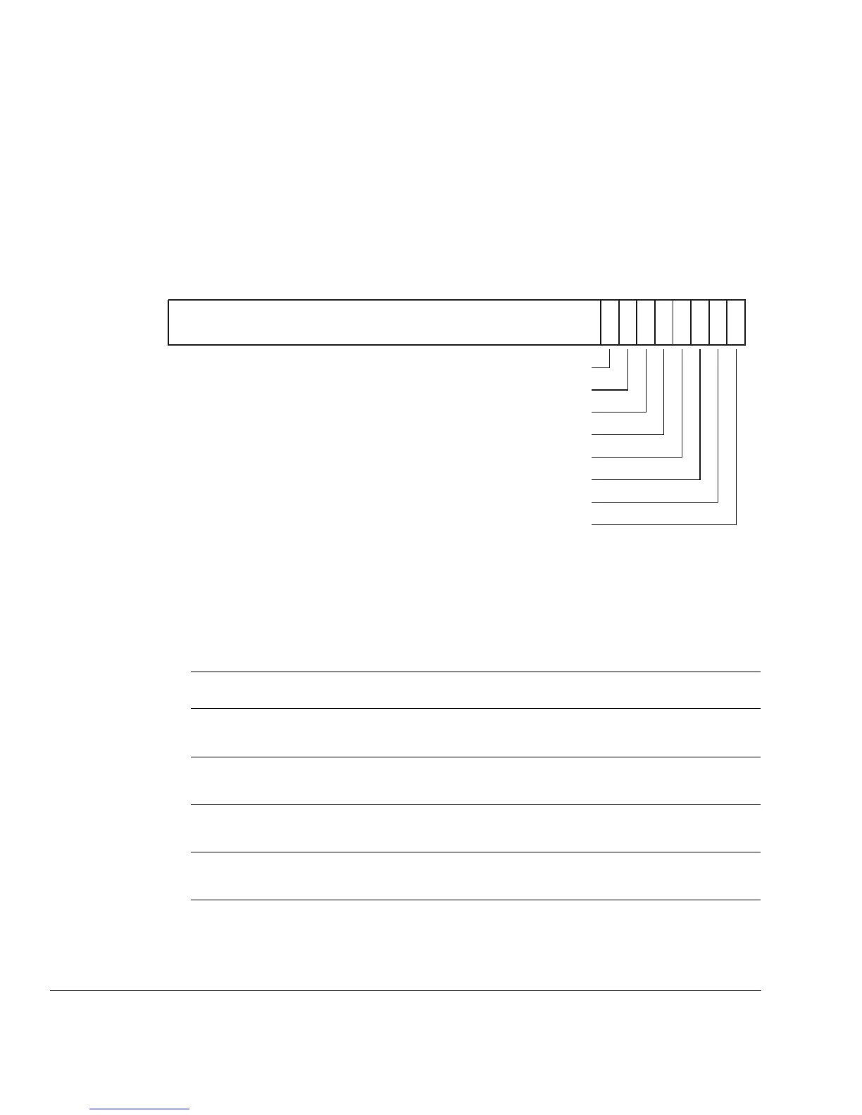
The MMU Debug Control Register format is shown in Figure B-8.
Figure B-8 MMU Debug Control Register format
The MMU Debug Control Register bit assignments are given in Table B-10. The reset
value of the MMU Debug Control Register is
0x0
.
6320
SBZ
DMTMD
45
DMTLI
DDUTM
1
DIUTL
DMTLD
DIUTM
DMTMI
DDUTL
731 8
Table B-10 MMU Debug Control Register bit assignments
Bit Name Function Description
[31:8] - Reserved Read = Unpredictable
Write = Should Be Zero
[7] DMTMI Disable main TLB matching for
instruction fetches
0 = Enable matching
1 = Disable matching
[6] DMTMD Disable main TLB matching for data
accesses
0 = Enable matching
1 = Disable matching
[5] DMTLI Disable main TLB load because of
instruction fetch miss
0 = Enable TLB load
1 = Disable TLB load
[4] DMTLD Disable main TLB load because of
data access miss
0 = Enable TLB load
1 = Disable TLB load

 Loading...

