CP15 Test and Debug Registers
B-6 Copyright © 2001-2003 ARM Limited. All rights reserved. ARM DDI0198D
Inserting or reading entries in the main TLB
Use this procedure to access entries in the main TLB:
1. Use the following Debug and Test Address Register instruction to access a main
TLB entry:
MCR p15, 0, <Rd>, c15, c1, 0 ; select TLB entry
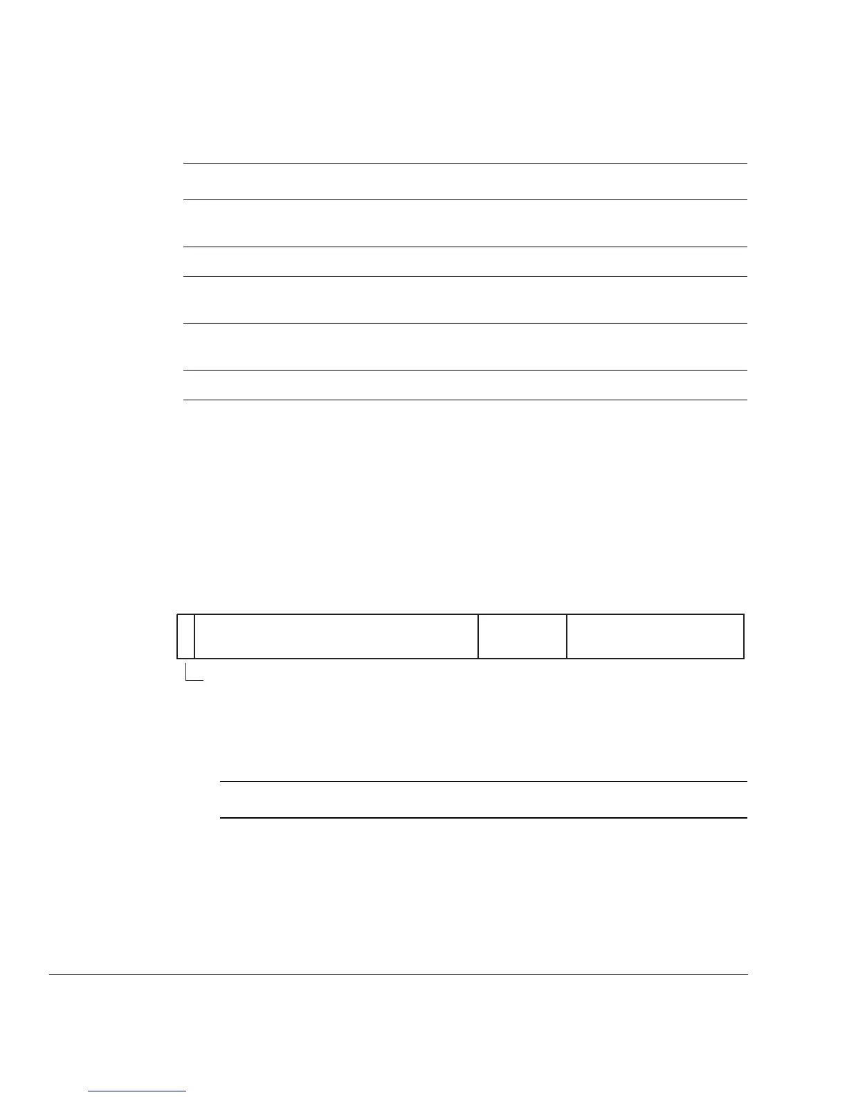
The Rd register selects the main TLB entry as Figure B-2 shows.
Figure B-2 Rd format for selecting main TLB entry
Table B-4 describes the Rd register entry-select bit fields.
MRC p15, 4/5, <Rd>, c15, c4, 0
MCR p15, 4/5, <Rd>, c15, c5, 0
Read PA and access permission data in main TLB entry
Write PA and access permission data data in main TLB entry
MCR p15, 4/5, <Rd>, c15, c7, 0
Transfer main TLB entry into RAM
MRC P15, 4/5, <Rd>, c15, c2, 1
MCR P15, 4/5, <Rd>, c15, c3, 1
Read tag in lockdown TLB entry
Write tag in lockdown TLB entry
MRC P15, 4/5, <Rd>, c15, c4, 1
MCR P15, 4/5, <Rd>, c15, c5, 1
Read PA and access permission data in lockdown TLB entry
Write PA and access permission data in lockdown TLB entry
MCR P15, 4/5, <Rd>, c15, c7, 1
Transfer lockdown TLB entry into RAM
Table B-3 MMU test operation instructions (continued)
Instruction Operation
31
Way
Indexed entry SBZSBZ
14 10 091530
Table B-4 Encoding of the main TLB entry-select bit fields
Bit Name Definition
[31] Way Way select:
1=way 1
0 = way 0.

 Loading...

