Programmer’s Model
2-28 Copyright © 2001-2003 ARM Limited. All rights reserved. ARM DDI0198D
The format of the Cache Lockdown Register L bits is shown in Table 2-21. All cache
ways are available for allocation from reset.
You can use the cache lockdown and cache unlock procedures described in:
• Specific loading of addresses into a cache way
• Cache unlock procedure on page 2-29.
Specific loading of addresses into a cache way
The procedure to lock down code and data into way i of a cache with N ways using
Format C involves making it impossible to allocate to any cache way other than the
target cache way:
1. Ensure that no processor exceptions can occur during the execution of this
procedure, for example by disabling interrupts. If this is not possible, all code and
data used by any exception handlers must be treated as code and data as in steps
2 and 3.
2. If an ICache way is being locked down, ensure that all the code executed by the
lockdown procedure is in an uncachable area of memory (including TCM) or in
an already locked cache way.
3. If a DCache way is being locked down, ensure that all data used by the lockdown
procedure is in an uncachable area of memory (including TCM) or is in an already
locked cache way.
4. Ensure that the data/instructions that are to be locked down are in a cachable area
of memory.
5. Ensure that the data/instructions that are to be locked down are not already in the
cache. Use the register c7 clean and/or invalidate operations to ensure this.
6. Write to register c9, CRm == 0, setting L==0 for bit i and L==1 for all other ways.
This enables allocation to the target cache way.
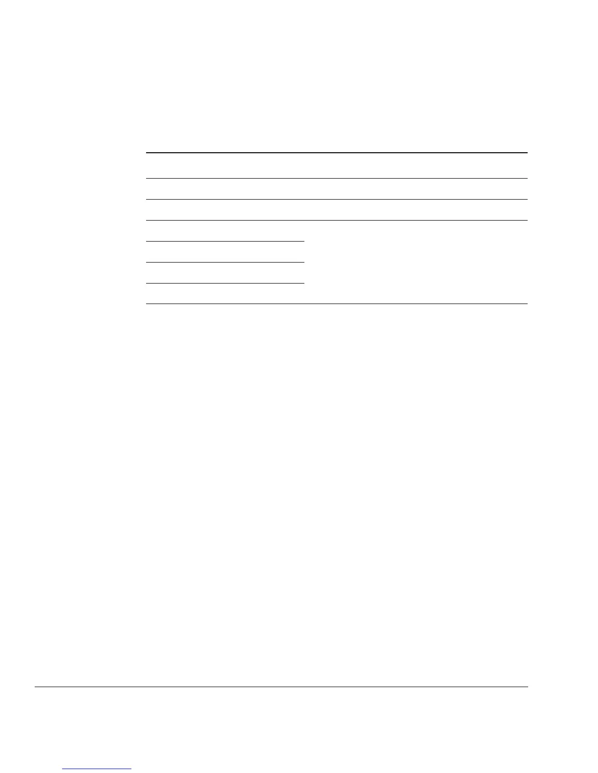
Table 2-21 Cache Lockdown Register L bits
Bits 4-way associative Notes
[31:16] UNP/SBZP Reserved
[15:4]
0xFFF
SBO
3 L bit for Way 3 Bits[3:0] are the L bits for each cache way:
0 = Allocation to the cache way is determined by the
standard replacement algorithm (reset state)
1 = No allocation is performed to this cache way.
2 L bit for Way 2
1 L bit for Way 1
0 L bit for Way 0
 Loading...


