3.1.5 System Bus (S—bus)
‘'N
The S-bus is a time-multiplexed address/data bus allowing communications between the system processing unit,
memory subsystem, I/O subsystem, and diagnostic subsystem. The bus is internal to the system board and consists
of a 32-bit, 3-state, bidirectional address/data bus, and the signals used to control, access, and permit transfers.
The S-bus supports multiple requestors with an address space of up to 128 megabytes. For each major clock cycle
of the VLSI chips (referred to as a T period), the 32-bit address/data bus has a defined addresstransfer time in
the first half of the T period and a data transfer time in the second half of the T period.
Figure 3-3 shows the S-bus and the elements that it connects.
3.1.6 Timing
For each 320 nanoseconds clock cycle (T period) of the VLSI chips, the 32-bit address/data bus has a defined
address transfer time in the first half of the
cycle
and a data transfer time in the second half of the cycle. To
prevent bus conflicts, successive address and data transfer times are separated by short intervals during which the
bus is in a high-impedance state. Most of the control for the bus comes from the basic system timing and from the
contents of the bus during the address phase. A special contrcil signal (READY) allows a bus transfer to continue
over consecutive cycles, and a bus-locking mechanism allows for indivisible read/modify/write operations.
3.1.7 Address Phase
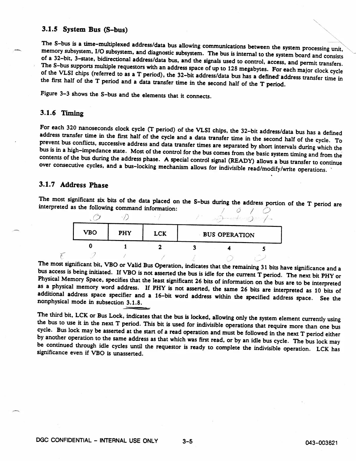
The most significant six bits of the data placed on the S-bus during the address portion of the T period are
interpreted as the following command information:
/
0
/ /-
_,")
;')
,,,
1
_
VBO
PHY
LCK
BUS OPERATION
0
1
2
3
4
5
_
The most significant bit, VBO or Valid Bus Operation, indicates that the remaining 31 bits have significance and a
bus access is being initiated. If VBO is not asserted the bus is idle for the current T period. The next bit PHY or
Physical Memory Space, specifies that the least significant 26 bits of information on the bus are to be interpreted
as a physical memory word address. If PHY is not asserted, the same 26 bits are interpreted as 10 bits of
additional address space specifier and a 16-bit word address within the specified address space. See the
nonphysical mode in subsection 3.1.8.
The third bit, LCK or Bus Lock, indicates that the bus is locked, allowing only the system element currently using
the bus to use it in the next T period. This bit is used for indivisible operations that require more than one bus
cycle. Bus lock may be asserted at the start of a read operation and must be followed in the next T period either
by another operation to the same address as that which was first read, or by an idle bus cycle. The bus lock may
be continued through idle cycles until the requestor is ready to complete the indivisible operation. LCK has
significance even if VBO is unasserted.
DGC CONFIDENTIAL - INTERNAL USE ONLY
3-5
043-003621