MB95630H Series
472 FUJITSU SEMICONDUCTOR LIMITED MN702-00009-2v0-E
CHAPTER 22 UART/SIO
22.6 Operations and Setting Procedure Example
● Reception in UART/SIO operation mode 1
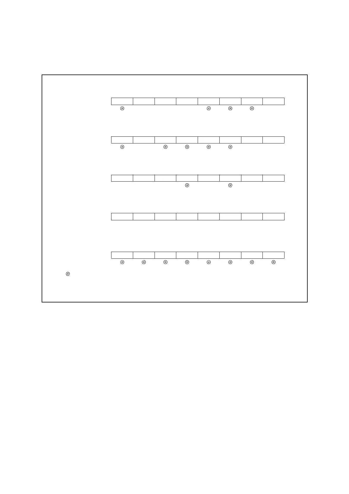
For reception in operation mode 1, each register is used as shown in Figure 22.6-11.
Figure 22.6-11 Registers Used for Reception in Operation Mode 1
The reception depends on whether the serial clock has been set to external or internal clock.
<When external clock is enabled>
When the reception operation enable bit (RXE) contains "1", serial data is received always at
the rising edge of the external clock signal.
<When internal clock is enabled>
The serial clock signal is output in accordance with transmission. Therefore, transmission
must be performed even when only performing reception. The following two procedures can
be used.
• Set the transmission operation enable bit (TXE) to "1", then write transmit data to the
UART/SIO serial output data register to generate the serial clock signal and start reception.
• Write transmit data to the TDRn register, then set the TXE bit to "1" to generate the serial
clock signal and start reception.
SMC1n (UART/SIO serial mode control register 1)
bit7 bit6 bit5 bit4 bit3 bit2 bit1 bit0
BDS PEN TDP SBL CBL1 CBL0 CKS MD
××× 1
SMC2n (UART/SIO serial mode control register 2)
bit7 bit6 bit5 bit4 bit3 bit2 bit1 bit0
SCKE TXOE RERC RXE TXE RIE TCIE TEIE
0 ××
SSRn (UART/SIO serial status and data register)
bit7 bit6 bit5 bit4 bit3 bit2 bit1 bit0
--PER OVE FER RDRF TCPL TDRE
××× × ××
TDRn (UART/SIO serial output data register)
bit7 bit6 bit5 bit4 bit3 bit2 bit1 bit0
TD7 TD6 TD5 TD4 TD3 TD2 TD1 TD0
××××××××
RDRn (UART/SIO serial input data register)
bit7 bit6 bit5 bit4 bit3 bit2 bit1 bit0
RD7 RD6 RD5 RD4 RD3 RD2 RD1 RD0
: Used bit
× : Unused bit
1 : Set to "1"
0 : Set to "0"