124©2018 Integrated Device Technology, Inc September 12, 2018
8A3xxxx Family Programming Guide
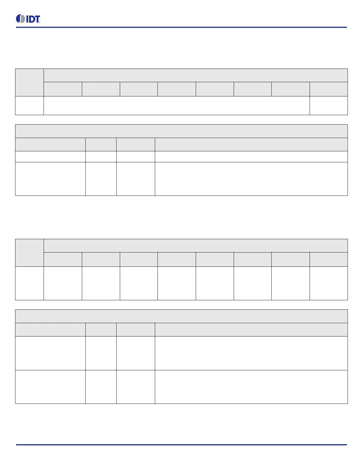
SYS_APLL.SYS_APLL_VREG_CTRL
VREG control register.
SYS_APLL.SYS_APLL_CP_CTRL_0
Sets the charge pump and 500uA enables for control 0.
Table 151: SYS_APLL.SYS_APLL_VREG_CTRL Bit Field Locations and Descriptions
Offset
Address
(Hex)
SYS_APLL.SYS_APLL_VREG_CTRL Bit Field Locations
D7 D6 D5 D4 D3 D2 D1 D0
004h RESERVED[7:1] VREG_VCAL
_0[0]
SYS_APLL.SYS_APLL_VREG_CTRL Bit Field Descriptions
Bit Field Name Field Type Default Value Description
RESERVED N/A - This field must not be modified from the read value
VREG_VCAL_0[0] R/W 0 VREG volt calibration control register bit 0.
When "1", PDCP and VCO regulators are set for 2.5V VDDA power supply
application. When "0" PDCP and VCO regulators are set for 3.3V VDDA
application.
Table 152: SYS_APLL.SYS_APLL_CP_CTRL_0 Bit Field Locations and Descriptions
Offset
Address
(Hex)
SYS_APLL.SYS_APLL_CP_CTRL_0 Bit Field Locations
D7 D6 D5 D4 D3 D2 D1 D0
005h CP_4_SS_E
NABLE[7]
CP_3_SS_E
NABLE[6]
CP_2_SS_E
NABLE[5]
CP_1_SS_E
NABLE[4]
SYS_APLL_
CP_4_SS_50
0U_ENABLE[
3]
SYS_APLL_
CP_3_SS_50
0U_ENABLE[
2]
SYS_APLL_
CP_2_SS_50
0U_ENABLE[
1]
SYS_APLL_
CP_1_SS_50
0U_ENABLE[
0]
SYS_APLL.SYS_APLL_CP_CTRL_0 Bit Field Descriptions
Bit Field Name Field Type Default Value Description
CP_4_SS_ENABLE[7] R/W 0 Enable source switching charge pump #4.
Must be low for 2.5V VDDA.
0 = disabled
1 = enabled.
CP_3_SS_ENABLE[6] R/W 0 Enable source switching charge pump #3.
Must be low for 2.5V VDDA.
0 = disabled
1 = enabled.
 Loading...