6©2018 Integrated Device Technology, Inc September 12, 2018
8A3xxxx Family Programming Guide
Example read from register 0xC024
B6* FC 00 C0 10 20 #Set Page Register, *I
2
C Address is left-shifted one bit.
B6 24* #Set I
2
C pointer to 0xC024, *I
2
C instruction should use “No Stop”
B7 <read back data> #Send address with Read bit set.
I
2
C 2-byte (2B) Addressing
8A3xxxx I
2
C 7-bit I
2
C address is 0x5B with LSB=R/W
Example Write “50” to register 0xCBE4
B6* FF FD 00 10 20 #Set Page Register, *I
2
C Address is left-shifted one bit.
B6 CB E4 50 #Write data to CB E4
Example read from register 0xC024:
B6* FF FD 00 10 20 #Set Page Register (*I
2
C Address is left-shifted one bit.)
B6 C0 24* #Set I
2
C pointer to 0xC024, *I
2
C instruction should use “No Stop”
B7 <read back data> #Send address with Read bit set.
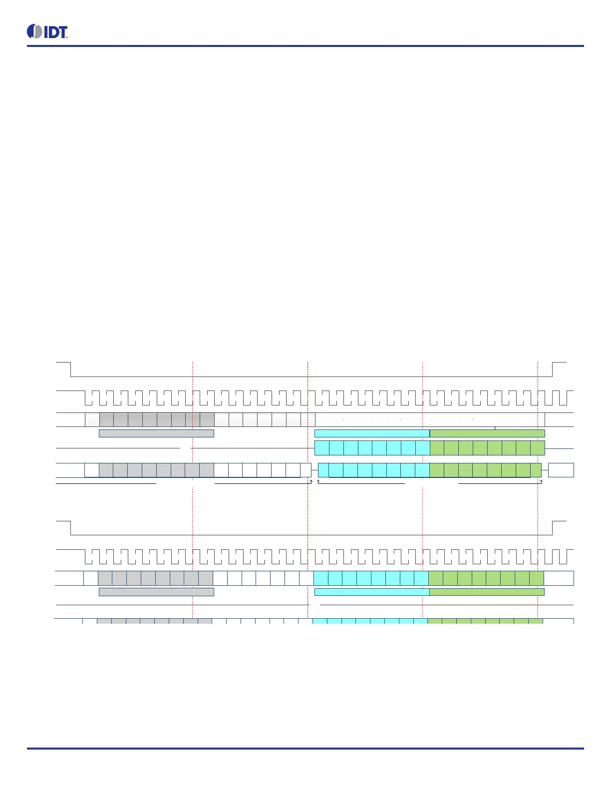
SPI Operation
The 8A3xxxx Family devices support SPI operation on their main and alternate serial ports. Figure 3 shows the sequencing of address and
data on the serial port in SPI mode.
Figure 3: SPI Sequencing Diagram
Each serial port can be independently configured for the following settings. These settings can come from register defaults or from an internal
OTP or external EEPROM configuration loaded at reset:
— 1-byte (1B) or 2-byte (2B) offset addressing (see Figure 1)
0 1 2 3 4 5 6 7 8 9 10 11 12 13 14 15 16 17 18 19 20 21 22 23 24 25 26 27 28 29 30 31
A14 A13 A12 A11 A10 A9 A8 A7 A6 A5 A4 A3 A2 A1 A0R/W
D0 D1 D2 D3 D4 D5 D6 D7 D0 D1 D2 D3 D4 D5 D6 D7
Hi-Z
CS
SCLK
SDI
(4-wire)
SDIO
(4-wire)
0 1 2 3 4 5 6 7 8 9 10 11 12 13 14 15 16 17 18 19 20 21 22 23 24 25 26 27 28 29 30 31
A0 A1 A2 A3 A4 A5 A6 A7 A8 A9 A10 A11 A12 A13 A14R/W
CS
SCLK
SDI
(4-wire)
SDIO
(4-wire)
D0 D1 D2 D3 D4 D5 D6 D7 D0 D1 D2 D3 D4 D5 D6 D7
Hi-Z
SPI Read Sequence*
SPI Write Sequence*
XX (SDI unused while data being read)
A14-A7 are omitted in 7b SPI Addressing Mode Data byte from Address provided Data byte from Address + 1
D7 D6 D5 D4 D3 D2 D1 D0 D7 D6 D5 D4 D3 D2 D1 D0
A14 A13 A12 A11 A10 A9 A8 A7 A6 A5 A4 A3 A2 A1 A0R/W D7 D6 D5 D4 D3 D2 D1 D0 D7 D6 D5 D4 D3 D2 D1 D0
A14-A7 are omitted in 7b SPI Addressing Mode Data byte from Address provided Data byte from Address + 1
* refer to timing diagrams for exact timing relationships
* refer to timing diagrams for exact timing relationships
SDIO
A0 A1 A2 A3 A4 A5 A6 A7 A8 A9 A10 A11 A12 A13R/W
SDIO
(3-wire)
D1 D2 D3 D4 D5 D6 D7 D0 D1 D2 D3 D4 D5 D6
A14 A13 A12 A11 A10 A9 A8 A7 A6 A5 A4 A3 A2 A1 A0R/W D7 D6 D5 D4 D3 D2 D1 D0 D7 D6 D5 D4 D3 D2 D1 D0
SDIO driven by Master SDIO driven by Slave