92©2018 Integrated Device Technology, Inc September 12, 2018
8A3xxxx Family Programming Guide
STATUS.DPLL0_PHASE_STATUS
Phase offset at output of decimator.
STATUS.DPLL1_PHASE_STATUS
Phase offset at output of decimator.
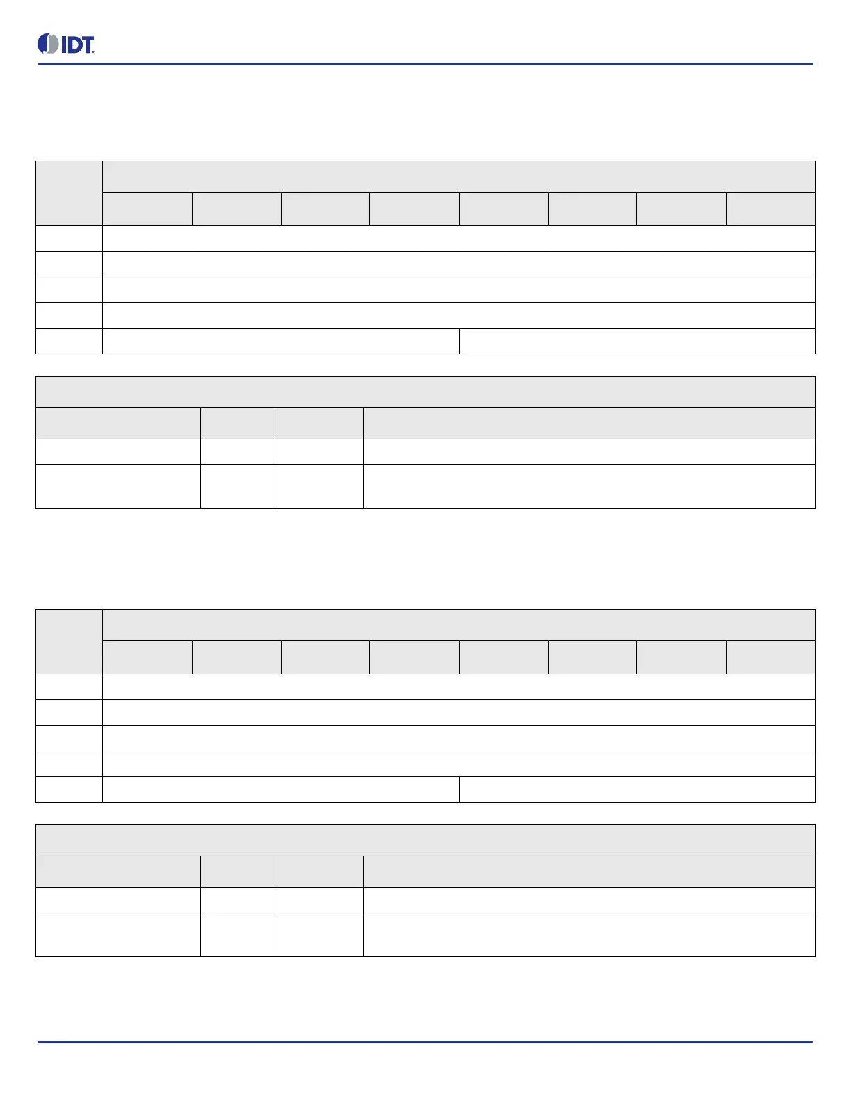
Table 103: STATUS.DPLL0_PHASE_STATUS Bit Field Locations and Descriptions
Offset
Address
(Hex)
STATUS.DPLL0_PHASE_STATUS Bit Field Locations
D7 D6 D5 D4 D3 D2 D1 D0
0DCh DPLL0_PHASE_STATUS[7:0]
0DDh DPLL0_PHASE_STATUS[15:8]
0DEh DPLL0_PHASE_STATUS[23:16]
0DFh DPLL0_PHASE_STATUS[31:24]
0E0h RESERVED[39:36] DPLL0_PHASE_STATUS[35:32]
STATUS.DPLL0_PHASE_STATUS Bit Field Descriptions
Bit Field Name Field Type Default Value Description
RESERVED N/A - This field must not be modified from the read value
DPLL0_PHASE_STATUS[
35:0]
R/O 0 Signed 36-bit phase offset in ITDC_UIs.
Table 104: STATUS.DPLL1_PHASE_STATUS Bit Field Locations and Descriptions
Offset
Address
(Hex)
STATUS.DPLL1_PHASE_STATUS Bit Field Locations
D7 D6 D5 D4 D3 D2 D1 D0
0E4h DPLL1_PHASE_STATUS[7:0]
0E5h DPLL1_PHASE_STATUS[15:8]
0E6h DPLL1_PHASE_STATUS[23:16]
0E7h DPLL1_PHASE_STATUS[31:24]
0E8h RESERVED[39:36] DPLL1_PHASE_STATUS[35:32]
STATUS.DPLL1_PHASE_STATUS Bit Field Descriptions
Bit Field Name Field Type Default Value Description
RESERVED N/A - This field must not be modified from the read value
DPLL1_PHASE_STATUS[
35:0]
R/O 0 Signed 36-bit phase offset in ITDC_UIs.