129©2018 Integrated Device Technology, Inc September 12, 2018
8A3xxxx Family Programming Guide
Module: INPUT_0
Input 0 configuration.
SYS_APLL.SYS_APLL_CTRL Bit Field Descriptions
Bit Field Name Field Type Default Value Description
VCCA_SEL[15] R/W 0 VCCA selection.
If SYS_APLL_CP_SS_CURRENT_1.GLOBAL_ENABLE is set to "0", this field
selects 2.5V or 3.3V VDDA operation with default charge pump values. If
SYS_APLL_CP_SS_CURRENT_1.GLOBAL_ENABLE is set to "1", this field will
be ignored and the charge pump fields can be programmed to customized
values.
0 = 3.3 V
1 = 2.5 V
DOUBLER_ENABLE[14] R/W 0 Enable the crystal input frequency doubler. Enable = 1.
Doubles the Input frequency of the SYS_APLL.
0 = disabled
1 = enabled
APLL_FBDIV_DIVIDER[13
:0]
R/W 0 Feedback divider value.
Sets the divider value of the feedback divider.
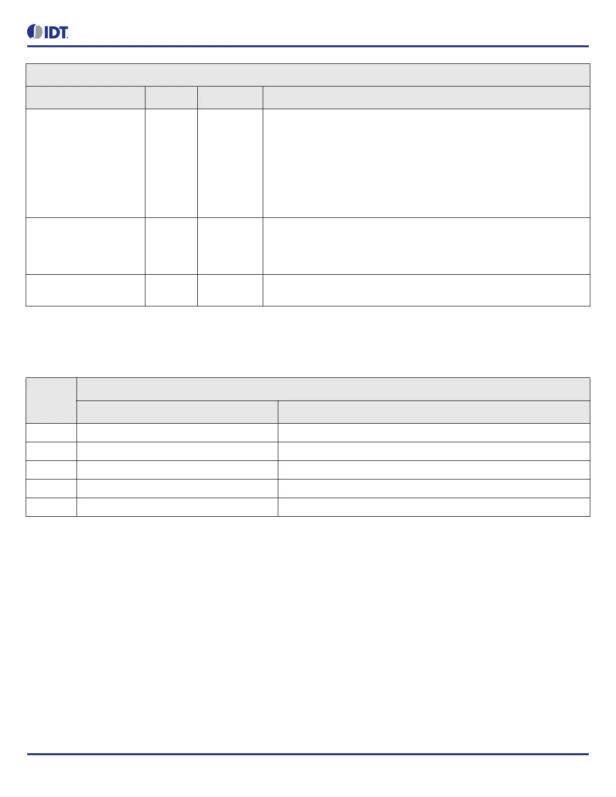
Table 157: INPUT_0 Register Index
Offset
(Hex)
Register Module Base Address: C1B0h
a
a. This register module is instantiated multiple times. This is the base address of the first instantiation of this module. For later instantiations,
use the appropriate module base address.
Individual Register Name Register Description
000h INPUT_0.IN_FREQ Input frequency in Hz.
008h INPUT_0.IN_DIV Input divider value.
00Ah INPUT_0.IN_PHASE Input phase offset configuration.
00Ch INPUT_0.IN_SYNC Frame pulse and sync pulse configuration.
00Dh INPUT_0.IN_MODE Input configuration.