334©2018 Integrated Device Technology, Inc September 12, 2018
8A3xxxx Family Programming Guide
BYTE.OTP_EEPROM_PWM_BUFF_115
-
BYTE.OTP_EEPROM_PWM_BUFF_116
-
BYTE.OTP_EEPROM_PWM_BUFF_117
-
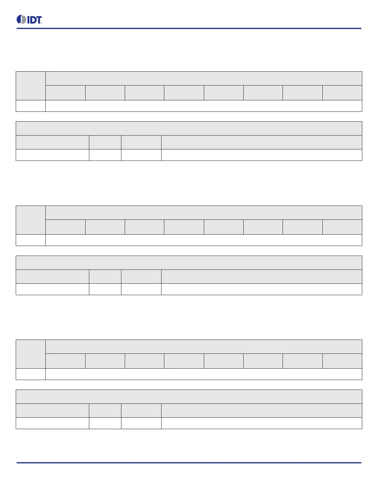
Table 515: BYTE.OTP_EEPROM_PWM_BUFF_115 Bit Field Locations and Descriptions
Offset
Address
(Hex)
BYTE.OTP_EEPROM_PWM_BUFF_115 Bit Field Locations
D7 D6 D5 D4 D3 D2 D1 D0
073h DATA[7:0]
BYTE.OTP_EEPROM_PWM_BUFF_115 Bit Field Descriptions
Bit Field Name Field Type Default Value Description
DATA[7:0] R/W 0 Data to be transferred into OTP, EEPROM or PWM.
Table 516: BYTE.OTP_EEPROM_PWM_BUFF_116 Bit Field Locations and Descriptions
Offset
Address
(Hex)
BYTE.OTP_EEPROM_PWM_BUFF_116 Bit Field Locations
D7 D6 D5 D4 D3 D2 D1 D0
074h DATA[7:0]
BYTE.OTP_EEPROM_PWM_BUFF_116 Bit Field Descriptions
Bit Field Name Field Type Default Value Description
DATA[7:0] R/W 0 Data to be transferred into OTP, EEPROM or PWM.
Table 517: BYTE.OTP_EEPROM_PWM_BUFF_117 Bit Field Locations and Descriptions
Offset
Address
(Hex)
BYTE.OTP_EEPROM_PWM_BUFF_117 Bit Field Locations
D7 D6 D5 D4 D3 D2 D1 D0
075h DATA[7:0]
BYTE.OTP_EEPROM_PWM_BUFF_117 Bit Field Descriptions
Bit Field Name Field Type Default Value Description
DATA[7:0] R/W 0 Data to be transferred into OTP, EEPROM or PWM.
 Loading...