231©2018 Integrated Device Technology, Inc September 12, 2018
8A3xxxx Family Programming Guide
DPLL_PHASE_PULL_IN_0.DPLL_PHASE_PULL_IN_CTRL
Phase pull-in configuration.
Module: GPIO_CFG
Global GPIO configuration.
GPIO_CFG.GPIO_CFG_GBL
Enable the gpio drive supply mode.
TRIGGER: Writing to this byte triggers a read and activation in hardware of all the bytes of the GPIO_DC_CFG module.
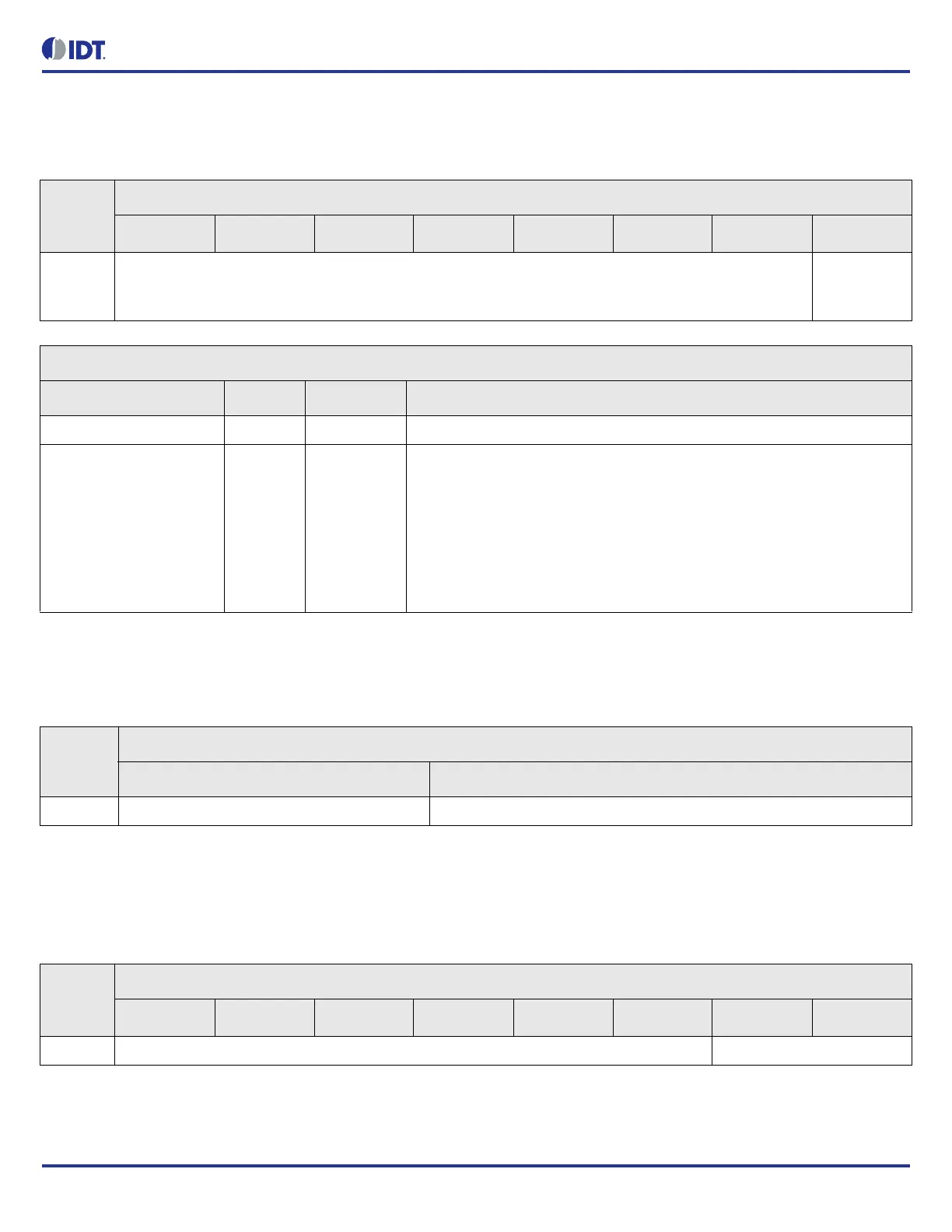
Table 299: DPLL_PHASE_PULL_IN_0.DPLL_PHASE_PULL_IN_CTRL Bit Field Locations and Descriptions
Offset
Address
(Hex)
DPLL_PHASE_PULL_IN_0.DPLL_PHASE_PULL_IN_CTRL Bit Field Locations
D7 D6 D5 D4 D3 D2 D1 D0
007h RESERVED[7:1] PHASE_PUL
L_IN_REQU
EST[0]
DPLL_PHASE_PULL_IN_0.DPLL_PHASE_PULL_IN_CTRL Bit Field Descriptions
Bit Field Name Field Type Default Value Description
RESERVED N/A - This field must not be modified from the read value
PHASE_PULL_IN_REQUE
ST[0]
R/W 0 Phase pull-in request.
Setting this bit to "1" starts a phase pull-in if there is no one in progress.
Otherwise, it will be ignored. Setting this bit to "0" terminates the on-going
phase pull-in. This request is only applicable to pll_mode: "write phase mode",
"write frequency mode", "GPIO inc/dec mode", and "synthesizer mode". It will
be ignored if the DPLL is in other modes. A pll-mode change will trigger a
termination of on-going phase pull-in. This bit will be self-cleared after the phase
pull-in finished.
Table 300: GPIO_CFG Register Index
Offset
(Hex)
Register Module Base Address: C8C0h
Individual Register Name Register Description
000h GPIO_CFG.GPIO_CFG_GBL Global GPIO parameters.
Table 301: GPIO_CFG.GPIO_CFG_GBL Bit Field Locations and Descriptions
Offset
Address
(Hex)
GPIO_CFG.GPIO_CFG_GBL Bit Field Locations
D7 D6 D5 D4 D3 D2 D1 D0
000h RESERVED[7:2] SUPPLY_MODE[1:0]
 Loading...