282©2018 Integrated Device Technology, Inc September 12, 2018
8A3xxxx Family Programming Guide
OUTPUT_TDC_0.OUTPUT_TDC_CTRL_4
Configure output TDC.
TRIGGER: Writing to this byte triggers a read and activation in hardware of all the bytes of the OUTPUT_TDC module.
OUTPUT_TDC_0.OUTPUT_TDC_CTRL_3 Bit Field Descriptions
Bit Field Name Field Type Default Value Description
TARGET_INDEX[7:4] R/W 0 Used in measurement mode to indicate the target clock.
Indicates the target to measure against 'source_index'.
0x0 = DPLL0
0x1 = DPLL1
0x2 = DPLL2
0x3 = DPLL3
0x4 = DPLL4
0x5 = DPLL5
0x6 = DPLL6
0x7 = DPLL7
0x8 = GPIO6
0x9 = GPIO1
0xA = GPIO2
0xB = GPIO7
SOURCE_INDEX[3:0] R/W 0 Used in measurement and alignment mode to indicate the source clock.
Indicates the source to be used as the measurement reference.
0x0 = DPLL0
0x1 = DPLL1
0x2 = DPLL2
0x3 = DPLL3
0x4 = DPLL4
0x5 = DPLL5
0x6 = DPLL6
0x7 = DPLL7
0x8 = GPIO6
0x9 = GPIO1
0xA = GPIO2
0xB = GPIO7
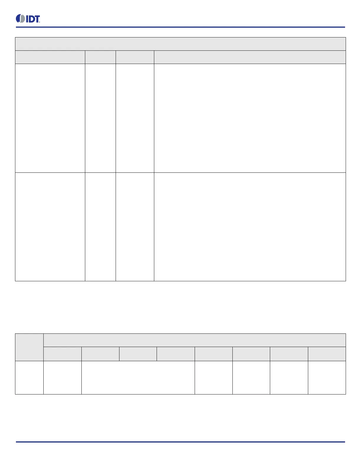
Table 381: OUTPUT_TDC_0.OUTPUT_TDC_CTRL_4 Bit Field Locations and Descriptions
Offset
Address
(Hex)
OUTPUT_TDC_0.OUTPUT_TDC_CTRL_4 Bit Field Locations
D7 D6 D5 D4 D3 D2 D1 D0
006h DISABLE_M
EASUREME
NT_FILTER[
7]
ALIGN_THRESHOLD_COUNT[6:4] ALIGN_RES
ET[3]
TYPE[2] MODE[1] GO[0]