181©2018 Integrated Device Technology, Inc September 12, 2018
8A3xxxx Family Programming Guide
SYS_DPLL.SYS_DPLL_CTRL_0
Reference switching configuration and forced lock reference selection.
SYS_DPLL.SYS_DPLL_UPDATE_RATE_CFG
System DPLL loop filter update rate configuration.
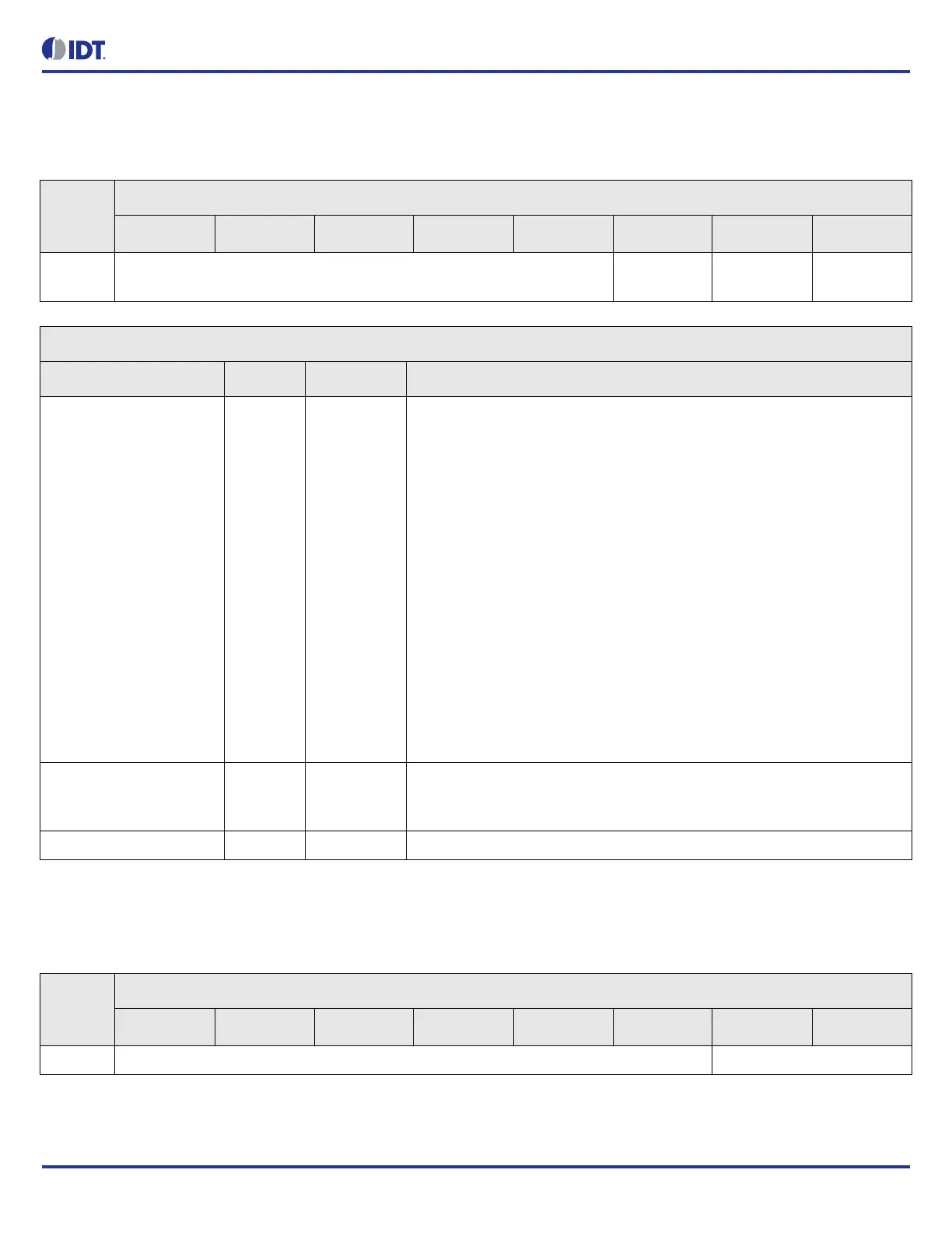
Table 222: SYS_DPLL.SYS_DPLL_CTRL_0 Bit Field Locations and Descriptions
Offset
Address
(Hex)
SYS_DPLL.SYS_DPLL_CTRL_0 Bit Field Locations
D7 D6 D5 D4 D3 D2 D1 D0
000h FORCE_LOCK_INPUT[7:3] RESERVED[
2]
REVERTIVE
_EN[1]
RESERVED[
0]
SYS_DPLL.SYS_DPLL_CTRL_0 Bit Field Descriptions
Bit Field Name Field Type Default Value Description
FORCE_LOCK_INPUT[7:3
]
R/W 0 System DPLL reference input index when force lock applied.
0x00 = CLK0
0x01 = CLK1
0x02 = CLK2
0x03 = CLK3
0x04 = CLK4
0x05 = CLK5
0x06 = CLK6
0x07 = CLK7
0x08 = CLK8
0x09 = CLK9
0x0A = CLK10
0x0B = CLK11
0x0C = CLK12
0x0D = CLK13
0x0E = CLK14
0x0F = CLK15
0x12 = XO_DPLL.
REVERTIVE_EN[1] R/W 0 Enable revertive mode.
0 = disabled
1 = enabled
RESERVED N/A - This field must not be modified from the read value
Table 223: SYS_DPLL.SYS_DPLL_UPDATE_RATE_CFG Bit Field Locations and Descriptions
Offset
Address
(Hex)
SYS_DPLL.SYS_DPLL_UPDATE_RATE_CFG Bit Field Locations
D7 D6 D5 D4 D3 D2 D1 D0
001h RESERVED[7:2] UPDATE_RATE_CFG[1:0]