38©2018 Integrated Device Technology, Inc September 12, 2018
8A3xxxx Family Programming Guide
STATUS.SER1_I2C_STATUS
Status of serial interface 1 I2C.
STATUS.IN0_MON_STATUS
Input 0 reference monitor status.
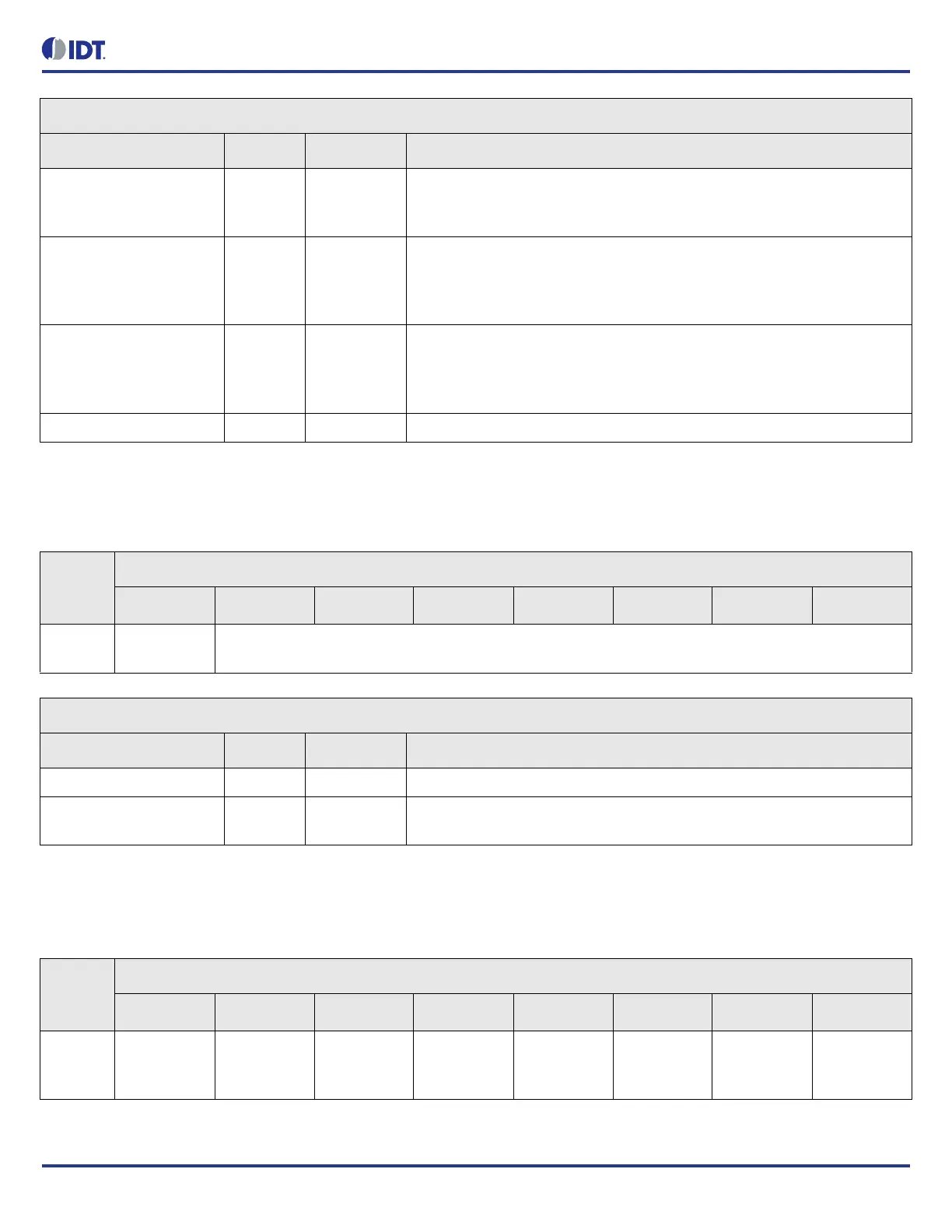
STATUS.SER1_SPI_STATUS Bit Field Descriptions
Bit Field Name Field Type Default Value Description
SPI_SDO_DELAY[4] R/O 0 SPI delay SDO driving edge.
0 = driving edge used for SDO
1 = SDO driving edge delayed half-cycle of SCLK
SPI_CLOCK_SELECTION[
3]
R/O 0 SPI Clock Selection for SDI sampling.
Indicates if the SPI clock selection is on a rising or falling edge.
0 = rising edge
1 = falling edge
SPI_DUPLEX_MODE[2] R/O 0 SPI 4-wire or 3-wire.
Indicates if the SPI is in full duplex or half duplex mode.
0 = full duplex
1 = half duplex
RESERVED N/A - This field must not be modified from the read value
Table 31: STATUS.SER1_I2C_STATUS Bit Field Locations and Descriptions
Offset
Address
(Hex)
STATUS.SER1_I2C_STATUS Bit Field Locations
D7 D6 D5 D4 D3 D2 D1 D0
007h RESERVED[
7]
DEVICE_ADDRESS[6:0]
STATUS.SER1_I2C_STATUS Bit Field Descriptions
Bit Field Name Field Type Default Value Description
RESERVED N/A - This field must not be modified from the read value
DEVICE_ADDRESS[6:0] R/O 0 I2C address of this I2C slave.
7-bit I2C address.
Table 32: STATUS.IN0_MON_STATUS Bit Field Locations and Descriptions
Offset
Address
(Hex)
STATUS.IN0_MON_STATUS Bit Field Locations
D7 D6 D5 D4 D3 D2 D1 D0
008h RESERVED[
7]
IN0_FREQ_
OFFS_LIM_
STICKY[6]
IN0_NO_AC
TIVITY_STIC
KY[5]
IN0_LOS_ST
ICKY[4]
RESERVED[
3]
IN0_FREQ_
OFFS_LIM_L
IVE[2]
IN0_NO_AC
TIVITY_LIVE
[1]
IN0_LOS_LI
VE[0]
 Loading...