6. Communication Protocol
6-12
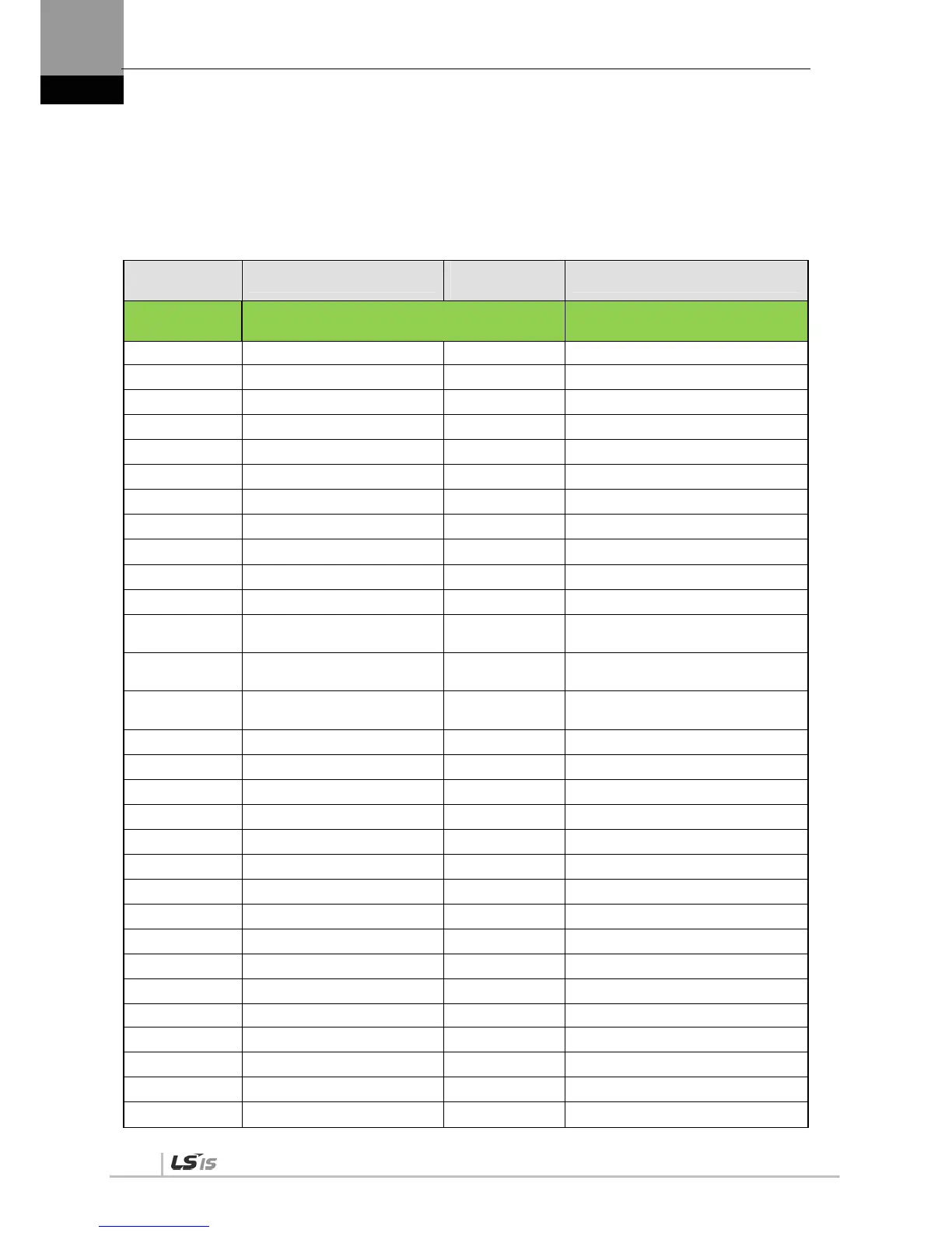
6.3.2 System Parameter Communication Address
Table
The following table lists Modbus communication addresses for the system parameter group
[P0-xx].
Communicatio
n Address
Parameter Name
Parameter
Number
Material Type
(Decimal
Number)
System Parameter Parameter
70 Motor ID P0 - 00 UINT16
72 Encoder Type P0 - 01 UINT16
74 Encoder pulse P0 - 02 UINT16
76 Select operation mode P0 - 03 UINT16
78 RS-422 communication speed P0 - 04 UINT16
80 System ID P0 - 05 UINT16
82 Main power input mode P0 - 06 UINT16
84 RST checking time P0 - 07 UINT16
86 Start-up display parameter P0 - 08 UINT16
88 Regenerative overload derating P0 - 09 UINT16
90 Regenerative resistance value P0 - 10 UINT16
92
Regenerative resistance
capacity
P0 - 11 UINT16
94
Overload detection base load
factor
P0 - 12 UINT16
96
Continuous overload warning
level
P0 - 13 UINT16
98 Encoder output pre-scale - L P0 - 14 INT32
100 Encoder output pre-scale - H
102 PWM OFF delay time P0 - 15 UINT16
104 Dynamic brake control mode P0 – 16 UINT16
106 Function setting bit P0 - 17 UINT16
108 DAC output mode P0 – 18 UINT16
110 DAC output offset 1 P0 - 19 INT16
112 DAC output offset 2 P0 - 20 INT16
114 Reserved P0 – 21
116 Reserved P0 – 22
118 DAC output scale 1 P0 – 23 UINT16
120 DAC output scale 2 P0 – 24 UINT16
122 Reserved P0 – 25
124 Reserved P0 - 26
126 U Phase Current Offset P0 - 27 INT16
128 V Phase Current Offset P0 - 28 INT16
 Loading...