Programming Model
http://www.motorola.com/computer/literature 3-35
3
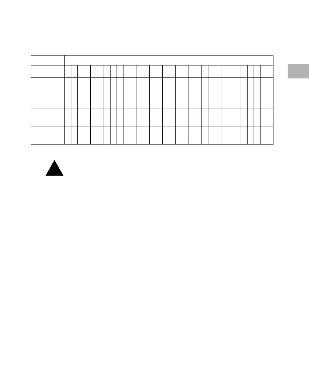
DRAM Attributes Register
!
Warning
To satisfy DRAM component requirements before the memory is used at
start-up, software must always wait at least 500µs between the initial
setting of a bank’s size bits, to a non-zero value, and the first accessing of
that bank. These settings are in the DRAM Attributes Register (offset
$FEF80010). The delay is intended to make sure that the bank has been
refreshed at least 8 times before it is used. The 500µs is sufficient as long
as the CLK Frequency Register (offset $FEF80020) is within a factor of 2
of matching the actual 60x clock frequency
ram a/b/c/d en ram a/b/c/d en enables accesses to the corresponding
block of DRAM when set, and disables them when cleared.
Address
$FEF80010
Bit
0
1
2
3
4
5
6
7
8
9
10
11
12
13
14
15
16
17
18
19
20
21
22
23
24
25
26
27
28
29
30
31
Name
ram a en
0
0
0
0
ram a siz0
ram a siz1
ram a siz2
ram b en
0
0
0
0
ram b siz0
ram b siz1
ram b siz2
ram c en
0
0
0
0
ram c siz0
ram c siz1
ram c siz2
ram d en
0
0
0
0
ram d siz0
ram d siz1
ram d siz2
Operation
R/W
R
R
R
R
R/W
R/W
R/W
R/W
R
R
R
R
R/W
R/W
R/W
R/W
R
R
R
R
R/W
R/W
R/W
R/W
R
R
R
R
R/W
R/W
R/W
Reset
0 PL
X
X
X
X
0 P
0 P
0 P
0 PL
X
X
X
X
0 P
0 P
0 P
0 PL
X
X
X
X
0 P
0 P
0 P
0 PL
X
X
X
X
0 P
0 P
0 P
 Loading...


