1-8 Computer Group Literature Center Web Site
Board Description and Memory Maps
1
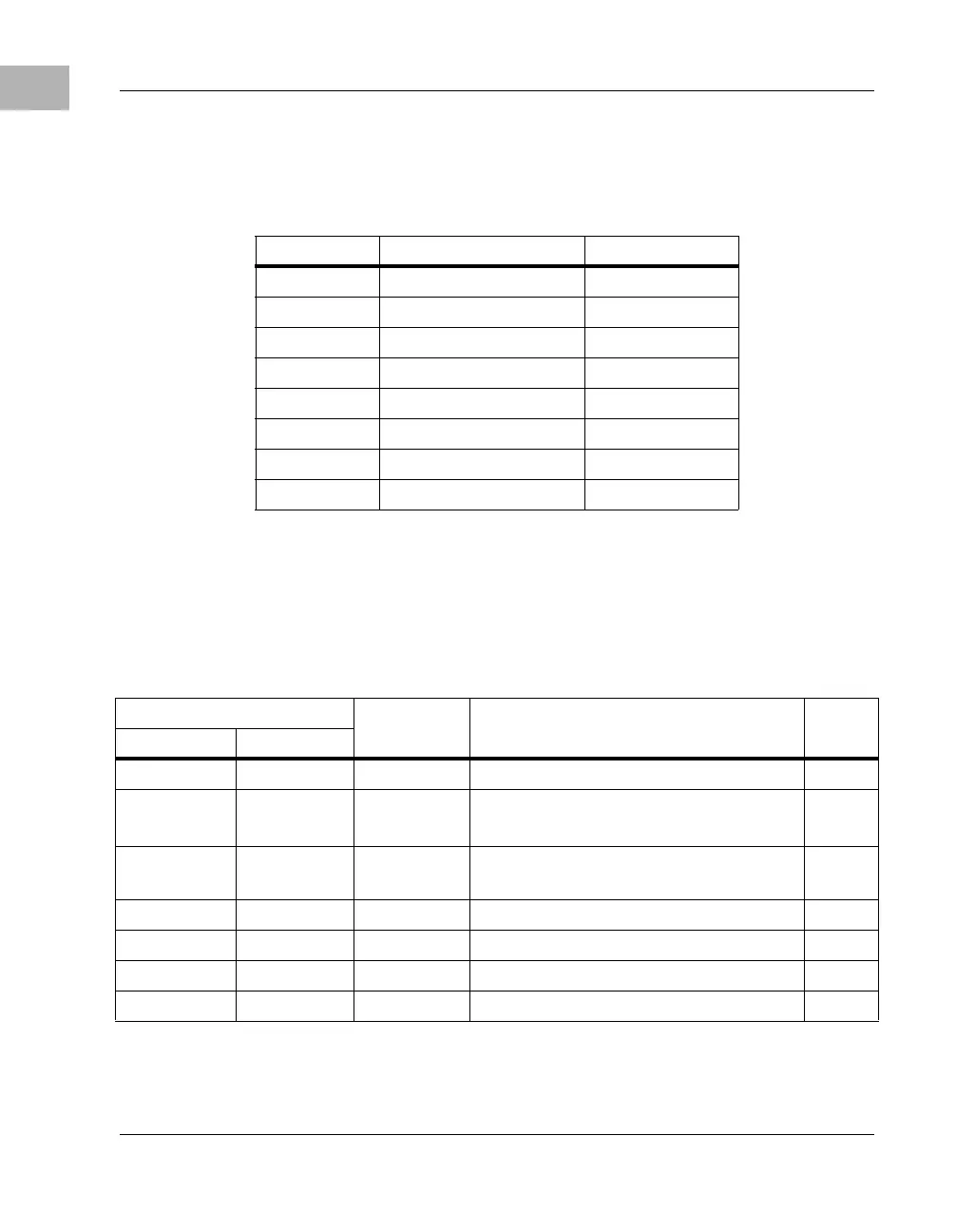
The following table shows the programmed values for the associated
Raven MPC registers for the processor CHRP memory map.
Processor PREP Memory Map
The Raven/Falcon chipset can be programmed for PREP-compatible
memory map. The following table shows the PREP memory map of the
MTX series from the point of view of the processor.
Table 1-4. Raven MPC Register Values for CHRP Memory Map
Address Register Name Register Value
FEFF 0040 MSADD0 4000 FCFF
FEFF 0044 MSOFF0 & MSATT0 0000 00C2
FEFF 0048 MSADD1 FD00 FDFF
FEFF 004C MSOFF1 & MSATT1 0300 00C2
FEFF 0050 MSADD2 0000 0000
FEFF 0054 MSOFF2 & MSATT2 0000 0002
FEFF 0058 MSADD3 FE00 FE7F
FEFF 005C MSOFF3 & MSATT3 0200 00C0
Table 1-5. PREP Memory Map Example
Processor Address Size Definition Notes
Start End
0000 0000 top_dram dram_size System Memory (onboard DRAM) 1
8000 0000 BFFF FFFF 1G Zero-Based PCI I/O Space:
0000 0000 - 3FFFF FFFF
2
C000 0000 FCFF FFFF 1G - 48M Zero-Based PCI/ISA Memory Space:
0000 0000 - 3CFFFFFF
2
FD00 0000 FEF7 FFFF 40.5M Reserved
FEF8 0000 FEF8 FFFF 64K Falcon Registers
FEF9 0000 FEFE FFFF 384K Reserved
FEFF 0000 FEFF FFFF 64K Raven Registers 5
 Loading...


