Programming Model
http://www.motorola.com/computer/literature 1-11
1
Notes
1. Programmable via the Raven’s PCI Configuration Registers.
The following table shows the programmed values for the associated
Raven PCI registers for the PCI CHRP memory map.
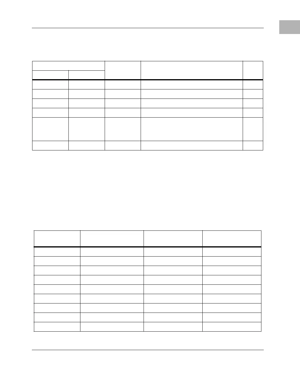
Table 1-7. PCI CHRP Memory Map Example
Processor Address Size Definition Notes
Start End
0000 0000 top_dram dram_size Onboard ECC DRAM 1
4000 0000 FBFF FFFF 3G - 64M PCI Memory Space 1
FC00 0000 FC03 FFFF 256K RavenMPIC 1
FC04 0000 FCFF FFFF 16M - 256K PCI Memory Space
FD00 0000 FDFF FFFF 16M PCI Memory Space or System Memory
Alias Space (mapped to 00000000 to
00FFFFFF)
1
FE00 0000 FFFF FFFF 32M Reserved
Table 1-8. Raven PCI Register Values for CHRP Memory Map
Configuration
Address Offset
Configuration
Register Name
Register Value
(Aliasing OFF)
Register Value
(Aliasing ON)
$14 RavenMPIC MBASE FC00 0000 FC00 0000
$80 PSADD0 0000 3FFF 0100 3FFF
$84 PSOFF0 & PSATT0 0000 00FX 0000 00FX
$88 PSADD1 0000 0000 FD00 FDFF
$8C PSOFF1 & PSATT1 0000 0000 0000 00FX
$90 PSADD2 0000 0000 0000 0000
$94 PSOFF2 & PSATT2 0000 0000 0000 0000
$98 PSADD3 0000 0000 0000 0000
$9C PSOFF3 & PSATT3 0000 0000 0000 0000
 Loading...


