Programming Model
http://www.motorola.com/computer/literature 1-9
1
Notes
1. Programmable via Falcon chipset.
2. Programmable via Raven ASIC.
3. The actual size of each ROM/FLASH bank may vary.
4. The first 1MB of ROM/FLASH Bank A appears at this range after
a reset if the rom_b_rv control bit is cleared. If the rom_b_rv
control bit is set then this address range maps to ROM/FLASH Bank
B.
5. The only method to generate a PCI Interrupt Acknowledge cycle
(8259 IACK) is to perform a read access to the Raven’s PIACK
register at 0xFEFF0030.
The following table shows the programmed values for the associated
Raven MPC registers for the processor PREP memory map.
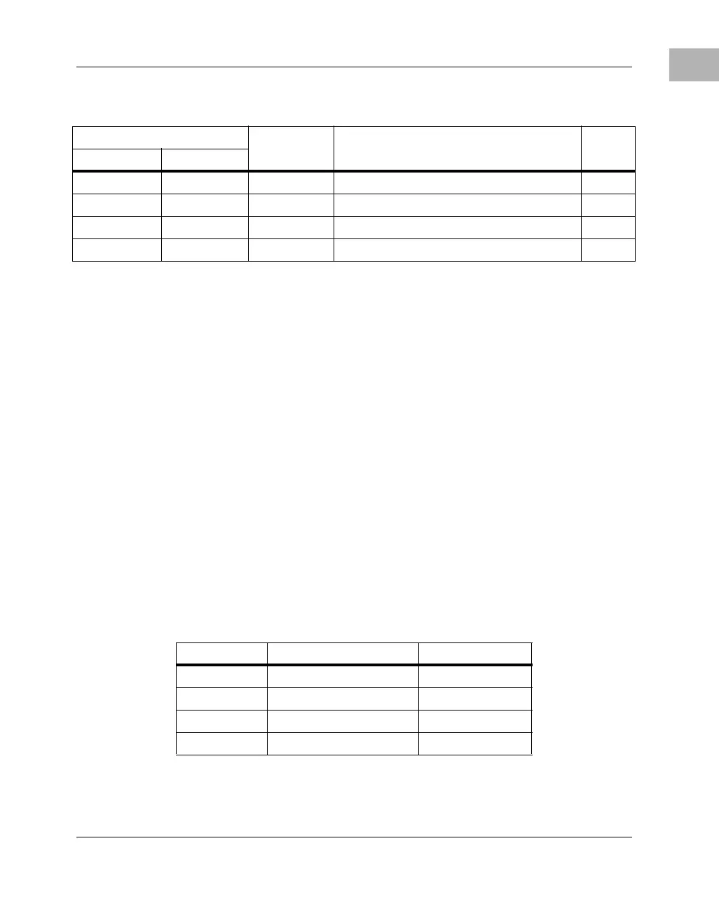
FF00 0000 FF7F FFFF 4M ROM/FLASH Bank A 1, 3
FF80 0000 FF8F FFFF 1M ROM/FLASH Bank B 1, 3
FF90 0000 FFEF FFFF 6M Reserved
FFF0 0000 FFFF FFFF 1M ROM/FLASH Bank A or Bank B 4
Table 1-6. Raven MPC Register Values for PREP Memory Map
Address Register Name Register Value
FEFF 0040 MSADD0 C000 FCFF
FEFF 0044 MSOFF0 & MSATT0 4000 00C2
FEFF 0048 MSADD1 0000 0000
FEFF 004C MSOFF1 & MSATT1 0000 0002
Table 1-5. PREP Memory Map Example (Continued)
Processor Address Size Definition Notes
Start End
 Loading...


