1-24 Computer Group Literature Center Web Site
Board Description and Memory Maps
1
PC87308VUL Super I/O Strapping
The PC87308VUL Super I/O provides the following functions to the MTX
series: a keyboard interface, a PS/2 mouse interface, a PS/2 floppy port,
two async serial ports and a parallel port. Refer to the PC87308VUL Data
Sheet for additional details and programming information.
The following table shows the hardware strapping for the Super I/O
device:
NVRAM/RTC & Watchdog Timer Registers
The MK48T59/559 provides the MTX series with 8KB of non-volatile
SRAM, a time-of-day clock, and a watchdog timer. Accesses to the
MK48T59/559 are accomplished via three registers: The NVRAM/RTC
Address Strobe 0 Register, the NVRAM/RTC Address Strobe 1 Register,
and the NVRAM/RTC Data Port Register. The NVRAM/RTC Address
Strobe 0 Register latches the lower 8 bits of the address and the
NVRAM/RTC Address Strobe 1 Register latches the upper 5 bits of the
address.
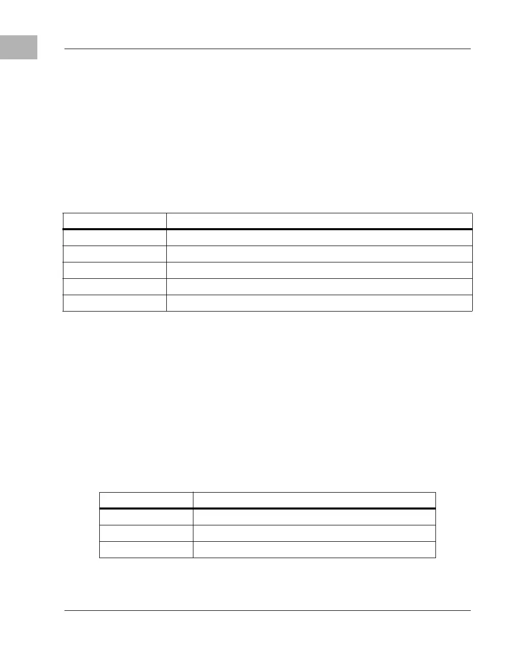
Table 1-14. Strap Pins Configuration for the PC87308VUL
Pins Reset Configuration
CFG0 0 - FDC, KBC and RTC wake up inactive.
CFG1 1 - Xbus Data Buffer (XDB) enabled.
CFG3, CFG2 00 - Clock source is 24MHz fed via X1 pin.
BADDR1, BADDR2 11 - PnP Motherboard, Wake in Config State. Index $002Eh.
SELCS 1 - CS0# on CS0# pin.
Table 1-15. MK48T59/559 Access Registers
PCI I/O Address Function
0000 0074 NVRAM/RTC Address Strobe 0 (A7 - A0)
0000 0075 NVRAM/RTC Address Strobe 1 (A15 - A8)
0000 0077 NVRAM/RTC Data Register
 Loading...


