Programming Model
http://www.motorola.com/computer/literature 3-37
3
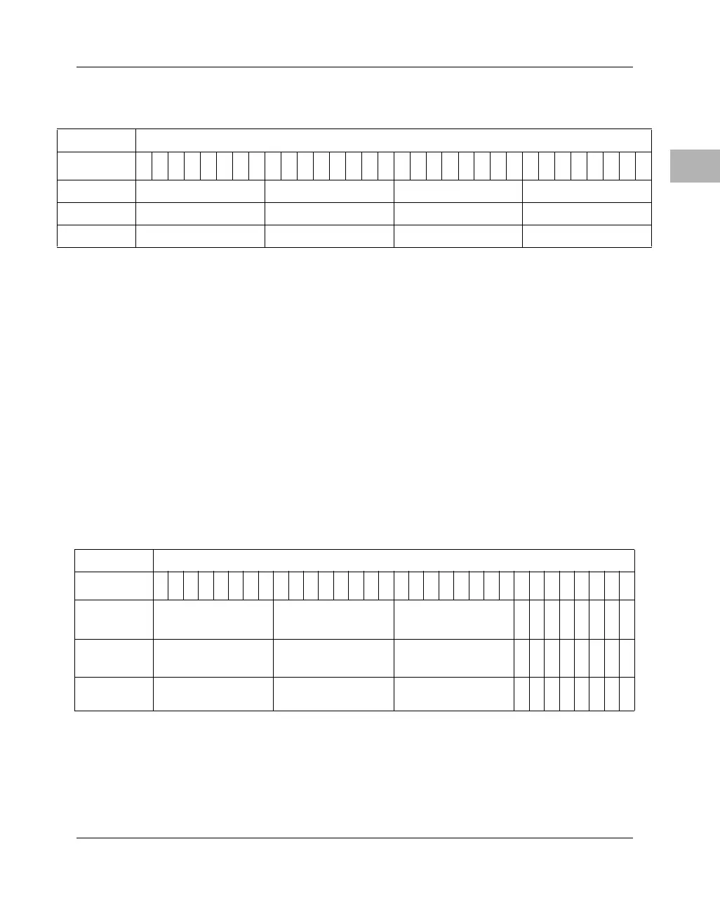
DRAM Base Register
RAM A/B/C/D BASE These control bits define the base address for their
block’s DRAM. RAM A/B/C/D BASE bits 0-7/8-15/16-23/24-31
correspond to PowerPC 60x address bits 0 - 7. For larger DRAM sizes, the
lower significant bits of A/B/C/D BASE are ignored. This means that the
block’s base address will always appear at an even multiple of its size.
Note Bit 0 is MSB.
Also note that the combination of RAM_X_BASE and
ram_x_siz should never be programmed such that DRAM
responds at the same address as the CSR, ROM/Flash, External
Register Set, or any other slave on the PowerPC bus.
CLK Frequency Register
CLK FREQUENCY These bits should be programmed with the
hexadecimal value of the operating CLOCK frequency in MHz (that is,
$42 for 66 MHz). When these bits are programmed this way, the chip’s
Address
$FEF80018
Bit
0
1
2
3
4
5
6
7
8
9
10
11
12
13
14
15
16
17
18
19
20
21
22
23
24
25
26
27
28
29
30
31
Name
RAM A BASE RAM B BASE RAM C BASE RAM D BASE
Operation
READ/WRITE READ/WRITE READ/WRITE READ/WRITE
Reset
0 PL 0 PL 0 PL 0 PL
Address
$FEF80020
Bit
0
1
2
3
4
5
6
7
8
9
10
11
12
13
14
15
16
17
18
19
20
21
22
23
24
25
26
27
28
29
30
31
Name
CLK
FREQUENCY
0
0
0
0
0
0
0
por
Operation
READ/WRITE READ ZERO READ ZERO
R
R
R
R
R
R
R
R/C
Reset
42 P X X
X
X
X
X
X
X
X
1 P
 Loading...


