1-6 Computer Group Literature Center Web Site
Board Description and Memory Maps
1
Notes
1. This default map for PCI/ISA I/O space allows software to
determine if the system is MPC105-based or Falcon/Raven-based
by examining either the PHB Device ID or the CPU Type Register.
2. The first 1MB of ROM/FLASH Bank A appears at this range after
a reset if the rom_b_rv control bit is cleared. If the rom_b_rv
control bit is set then this address range maps to ROM/FLASH Bank
B.
Processor CHRP Memory Map
The following table shows a recommended CHRP memory map from the
point of view of the processor.
FEF9 0000 FEFE FFFF 384K Not mapped
FEFF 0000 FEFF FFFF 64K Raven Registers
FF00 0000 FFEF FFFF 15M Not mapped
FFF0 0000 FFFF FFFF 1M ROM/FLASH Bank A or Bank B 2
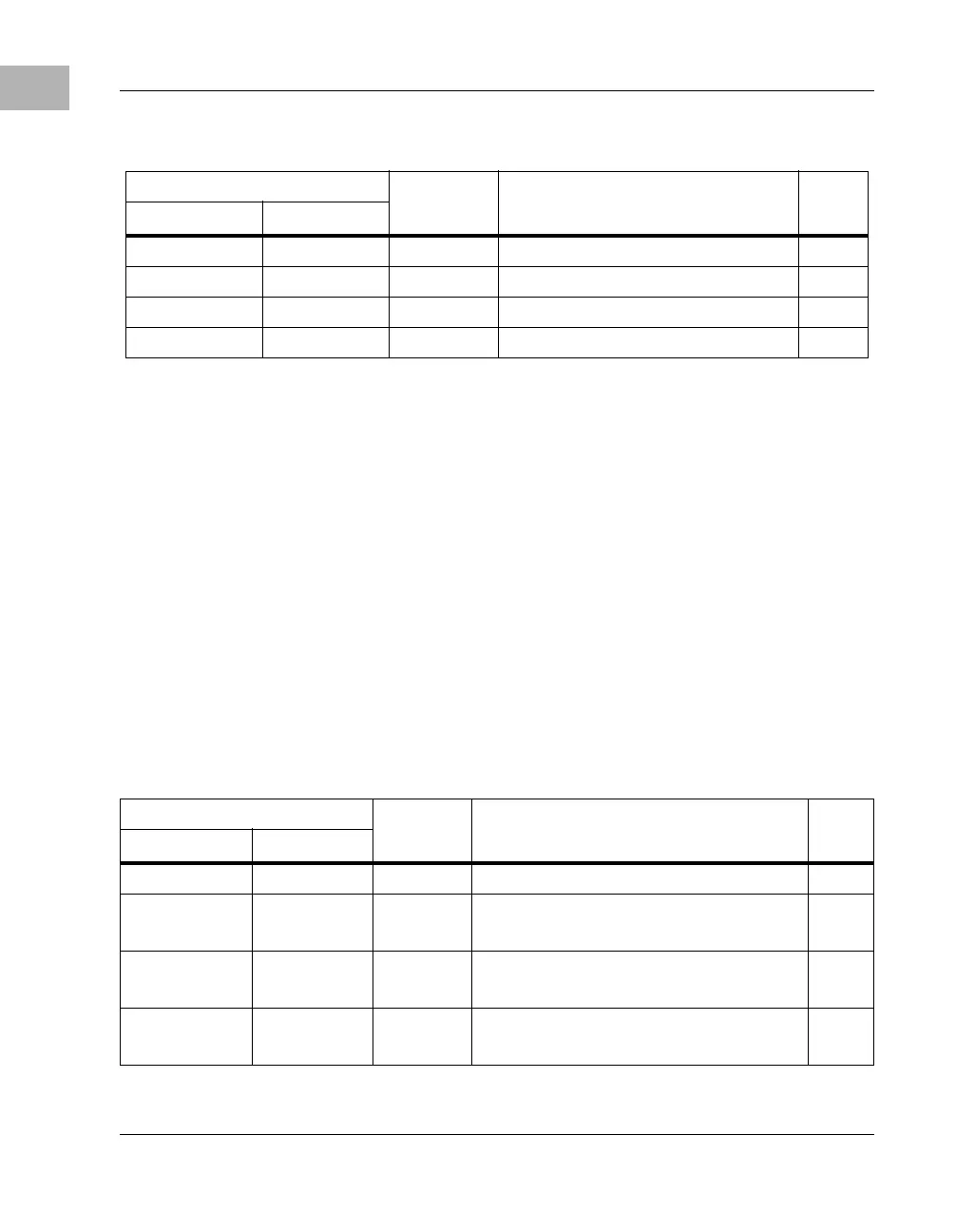
Table 1-3. CHRP Memory Map Example
Processor Address Size Definition
Notes
Start End
0000 0000 top_dram dram_size System Memory (onboard DRAM) 1, 2
4000 0000 FCFF FFFF 3G - 48M PCI Memory Space:
4000 0000 to FCFF FFFF
3,4
FD00 0000 FDFF FFFF 16M Zero-Based PCI/ISA Memory Space
(mapped to 00000000 to 00FFFFFF)
3
FE00 0000 FE7F FFFF 8M Zero-Based PCI/ISA I/O Space
(mapped to 00000000 to 007FFFFF)
3,5
Table 1-2. Default Processor Memory Map (Continued)
Processor Address Size Definition
Notes
Start End
 Loading...


